Thick film dielectric structure for thick dielectric electroluminescent displays

a dielectric structure and electroluminescent display technology, applied in the direction of discharge tube luminescnet screens, discharge tube/lamp details, coatings, etc., can solve the problems of film dielectric layer still having residual porosity, overlayer not completely filling the porosity of sintered material, and increasing the display area. , to achieve the effect of reducing the density of surface defects, improving the smoothing layer, and facilitating wetting of the underlying

Inactive Publication Date: 2010-06-22
IFIRE IP CORP
View PDF17 Cites 9 Cited by
  • Summary
  • Abstract
  • Description
  • Claims
  • Application Information

AI Technical Summary

Benefits of technology

[0009]The invention is an improved smoothing layer that is applied onto a thick film dielectric layer forming a composite. The improved smoothing layer results in substantially reduced density of surface defects in the base thick film dielectric layer. The improvement is achieved by incorporating a surfactant within the smoothing layer. The addition of surfactant to the deposition solution forming the smoothing layer facilitates wetting of the underlying thick film dielectric layer and thus a reduction in the pores / holes (herein referred to as defects) present in the thick film dielectric layer.
[0017]an upper smoothing layer, wherein said smoothing layer reduces defects in said lower thick film dielectric layer, said smoothing layer being made by the addition of a surfactant to a metal organic solution or sol gel that is subsequently applied to the thick film dielectric layer and sintered.

Problems solved by technology

However, the overlayer does not completely fill the porosity of the sintered material since it undergoes a severe volume reduction when the sol gel or MOD precursor materials are fired to form the piezoelectric or ferroelectric material.
Dielectric breakdown is associated with random defects in the dielectric layers and the probability of breakdown increases with increasing display area.
However, the modified thick film dielectric layer still contains residual porosity.

Method used


Image

  • Thick film dielectric structure for thick dielectric electroluminescent displays
  • Thick film dielectric structure for thick dielectric electroluminescent displays
  • Thick film dielectric structure for thick dielectric electroluminescent displays

Examples


example 1

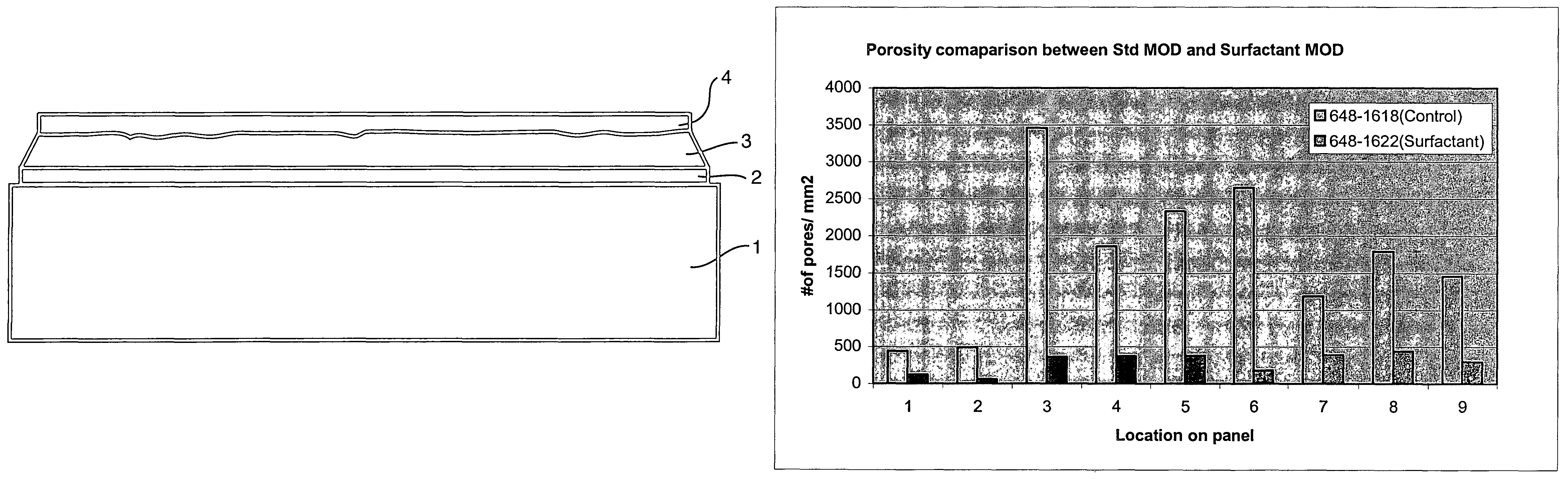
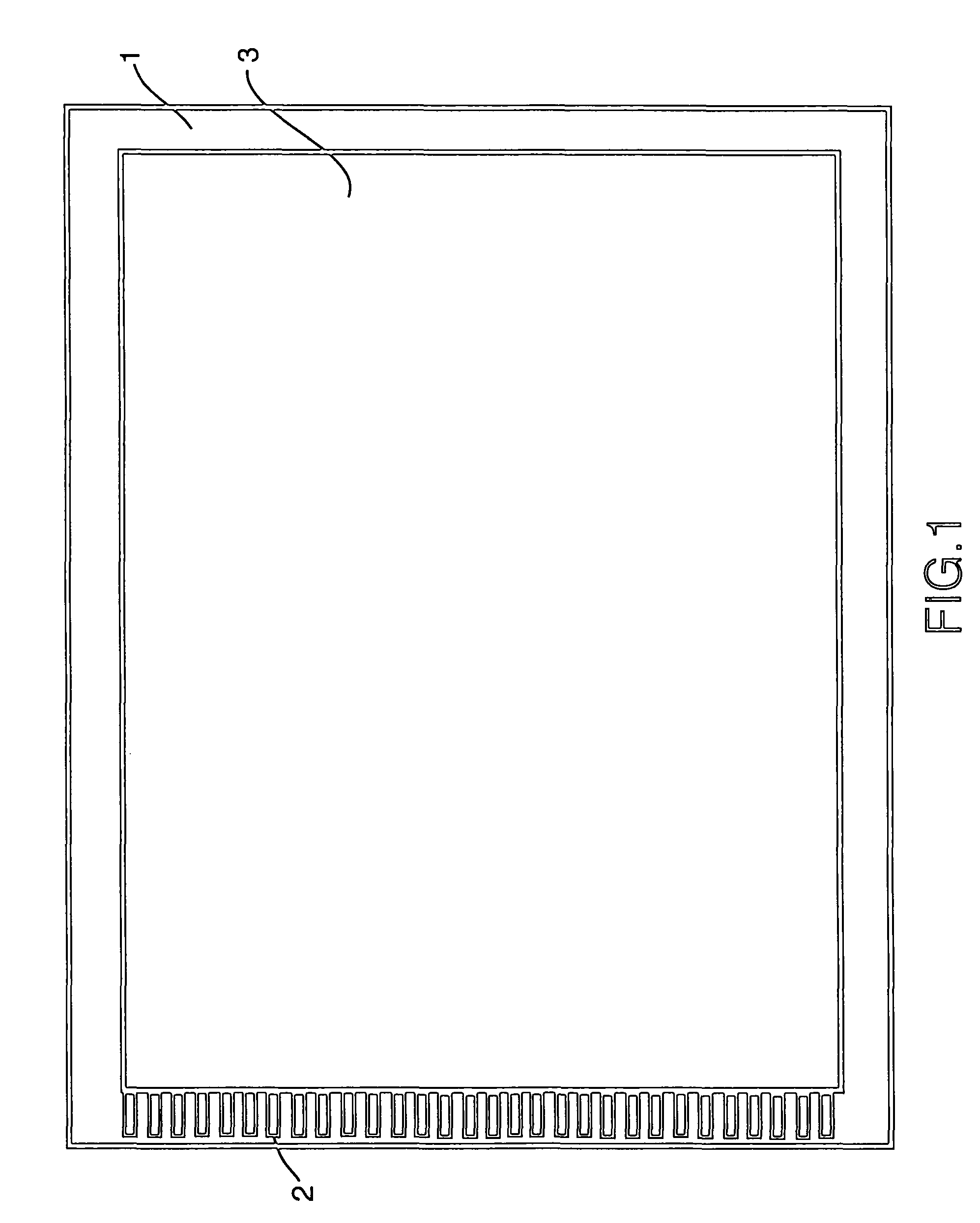
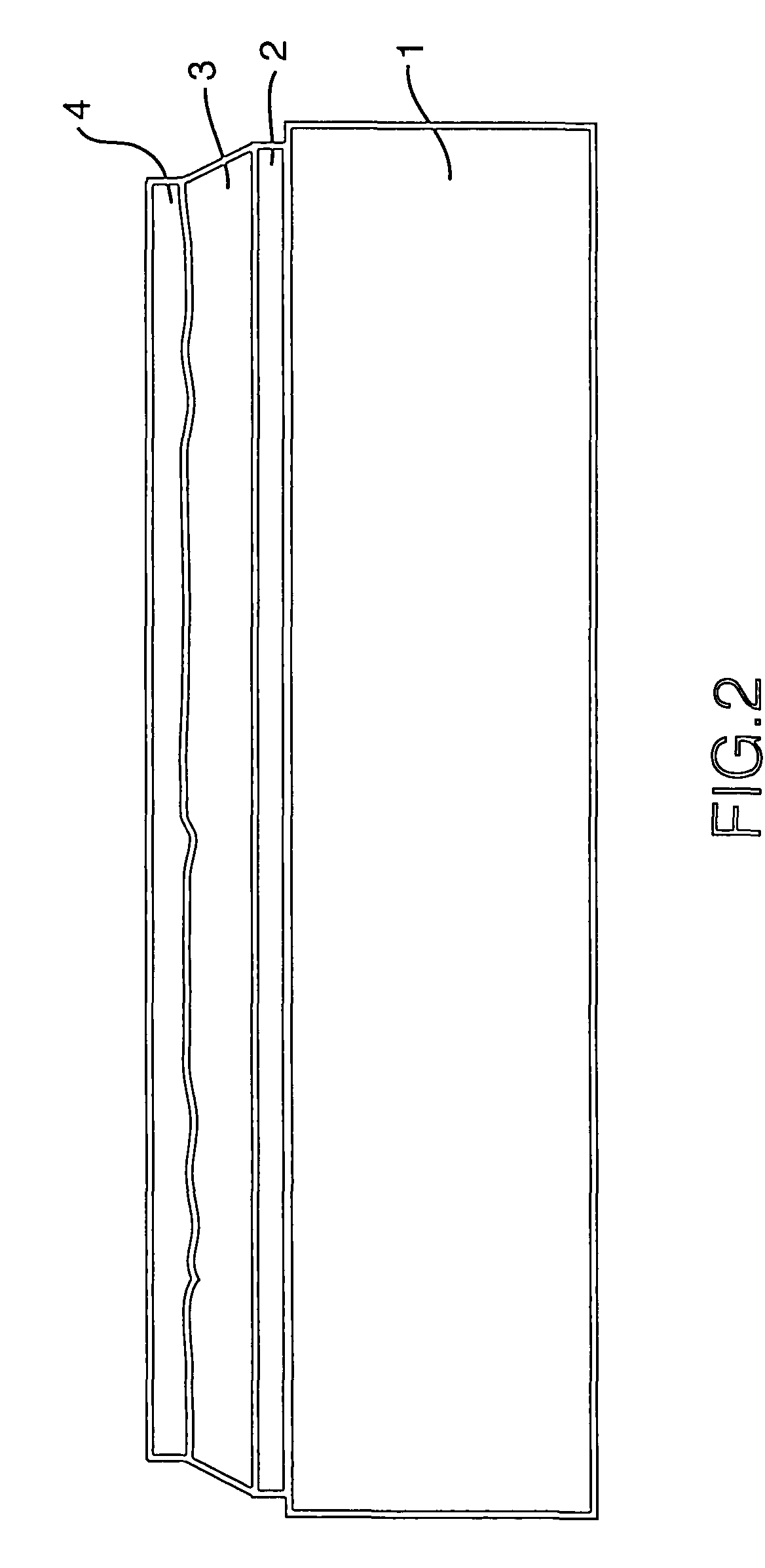
[0059]With reference to the schematic diagrams of FIG. 1 and FIG. 2, a set of gold row electrodes 2 and a thick film dielectric layer 3 for a 43 centimeter diagonal electroluminescent display were constructed on a PP8C glass substrate 1 obtained from Nippon Electric Glass Co. Ltd. of Osaka Japan. The methods for deposition of the row electrodes and the thick dielectric layer were similar to the methods described in U.S. patent application Ser. No. 09 / 326,777 in combination with the methods described herein. The gold electrode layer was deposited onto the substrate prior to deposition of a thick film dielectric layer. The thick film dielectric layer was formed of two sequentially formed layers with the process for depositing each layer consisting of printing a thick film paste, drying the printed layer, densifying the printed layer using isostatic pressing and finally sintering the densified layer. The densification process was carried out using cold isostatic pressing as taught in U...

example 2

[0062]A composite thick dielectric structure was constructed on a substrate similar to that described in example 1, except that a MOD solution without surfactant added and with a viscosity of 15 to 40 centipoise was used in place of the MOD solution for the first MOD layer as described in Example 1.

[0063]The surface of the completed composition dielectric layer was examined under a microscope. A photomicrograph of the surface is shown in FIG. 4. The areal density of defects is about 3500 defects per square centimeter. Compared to the surface shown in FIG. 3, the surface of the MOD layer shows a large number of defects (pits and indentations) evident in the photomicrograph, showing the utility of the surfactant containing MOD solution described in example 1 in dramatically reducing the number of surface defects. FIG. 5 shows a histogram with the number of defects for several 0.15 square millimeter sections of a thick dielectric layer made according to the method of the prior art with...


PUM

PropertyMeasurementUnit
dielectric constantaaaaaaaaaa
temperaturesaaaaaaaaaa
total thicknessaaaaaaaaaa

Abstract

An improved smoothing layer for use with a thick film dielectric layer, and improved composite thick film dielectric structure is provided. The smoothing layer is a piezoelectric or ferroelectric material that has a reduced amount of defects. The smoothing layer is formed by the addition of surfactant to a sol gel or metal organic solution of organo metallic precursor compounds. The composite thick film dielectric structure comprises a thick film dielectric composition having a PZT smoothing layer thereon, the smoothing layer being made by a process incorporating surfactant. Both the smoothing layer and the composite thick film dielectric structure are for use in electroluminescent displays.

Description

[0001]This application claims the benefit of U.S. Provisional Application Ser. No. 60 / 560,602, filed Apr. 9, 2004.FIELD OF THE INVENTION[0002]The invention relates generally to thick film dielectric electroluminescent displays. More specifically, the invention is an improved novel composite thick film dielectric structure, a method of making thereof and electroluminescent displays incorporating such structures.BACKGROUND OF THE INVENTION[0003]Thick film dielectric electroluminescent displays are typically fabricated on ceramic, glass ceramic, glass or other heat resistant substrate and provide superior resistance to dielectric breakdown, as well as a reduced operating voltage compared to thin film electroluminescent (TFEL) displays fabricated on glass substrates. The fabrication process for the display entails first depositing a set of row electrodes on the substrate. Next a thick film dielectric layer is deposited, following this, a thin film structure is deposited that comprises o...

Claims


Application Information

Patent Timeline
Patent Type & Authority Patents(United States)
IPC IPC(8): H05B33/10C03C8/14C03C17/36H01L21/469H05B33/22
CPCC03C17/36C03C17/3642C03C17/3649C03C17/3655C03C17/3657H05B33/22H05B33/10C03C17/3671C03C2217/40C03C2218/116C03C2218/119
Inventor MAHMOOD, KIFAH KAMILLEE, GANGOKPUGLIESE, VINCENT JOSEPH ALFRED
Owner IFIRE IP CORP
Why Eureka
Try Eureka