Solid-state imaging element and method for manufacturing the same
a solid-state imaging and element technology, applied in the field of resonance-type solid-state imaging elements, can solve the problems of manufacturing cost and cost, and the difficulty of providing sensitivity to light having such a long wavelength to an image sensor using a silicon substrate, and achieve the effects of low cost, high sensitivity and high sensitivity
- Summary
- Abstract
- Description
- Claims
- Application Information
AI Technical Summary
Benefits of technology
Problems solved by technology
Method used
Image

Examples
embodiment 1
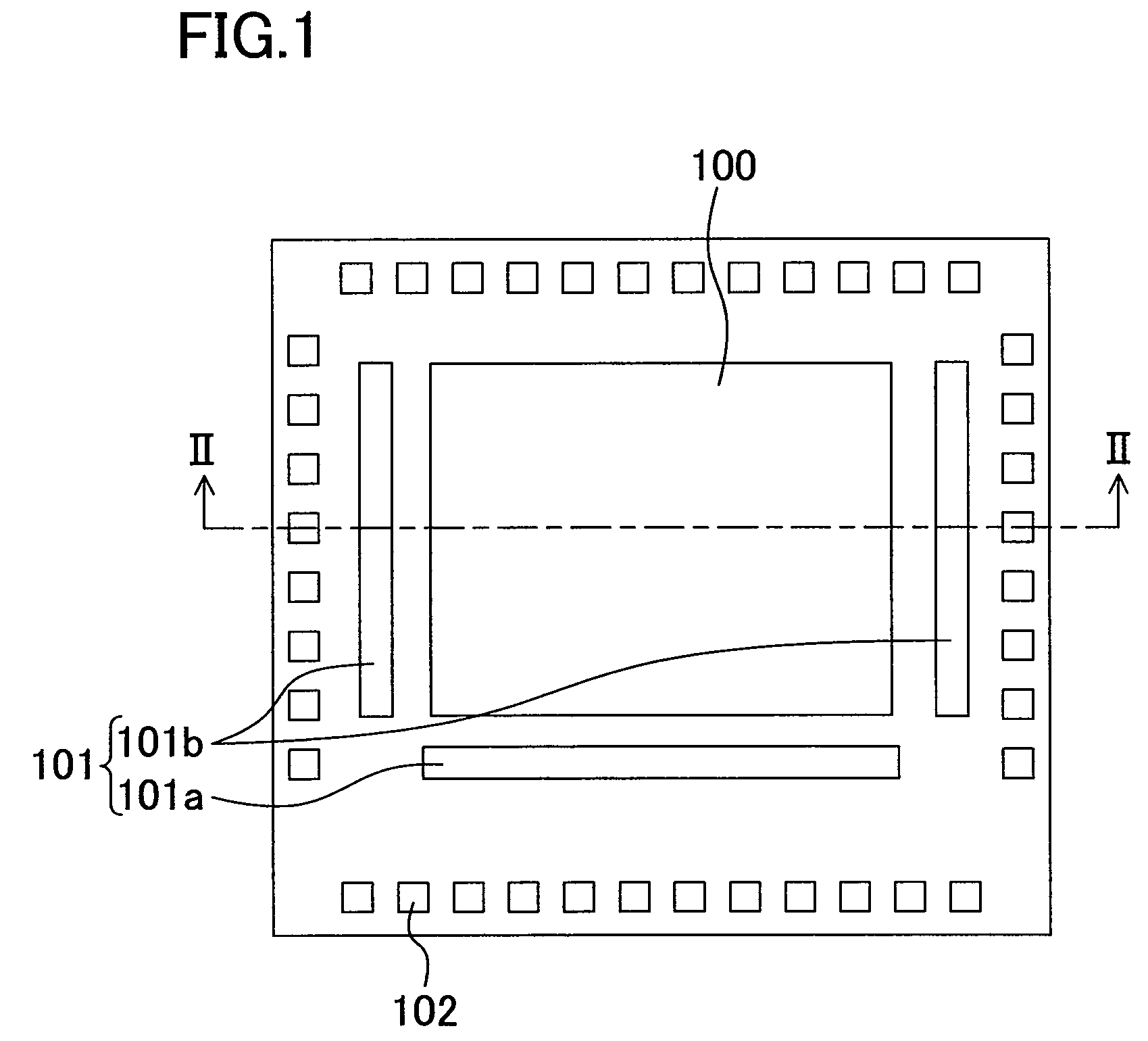
[0033]FIG. 1 is a schematic plan view for explaining an overall structure of a resonance type solid-imaging element in accordance with Embodiment 1 of the present invention. FIG. 1 is a view as viewed from the obverse face side of a substrate (a face where semiconductor elements are formed).
[0034]As shown in FIG. 1, the solid-state imaging element of the present embodiment includes an imaging region 100 and a peripheral circuit region 101. In the imaging region 100, a plurality of pixels for photoelectric conversion are arranged in matrix. The peripheral circuit region 101 is arranged around the imaging region 100 and includes various circuits relating to signal reading, such as a vertical shift resistor 101b for selecting a pixel from which a signal is to be read out, a horizontal shift resistor 101a for outputting a signal read out from a pixel to the outside of the solid-state imaging element, and the like.
[0035]Bonding pads 102 made of metal, such as aluminum, aluminum alloy, or...
embodiment 2
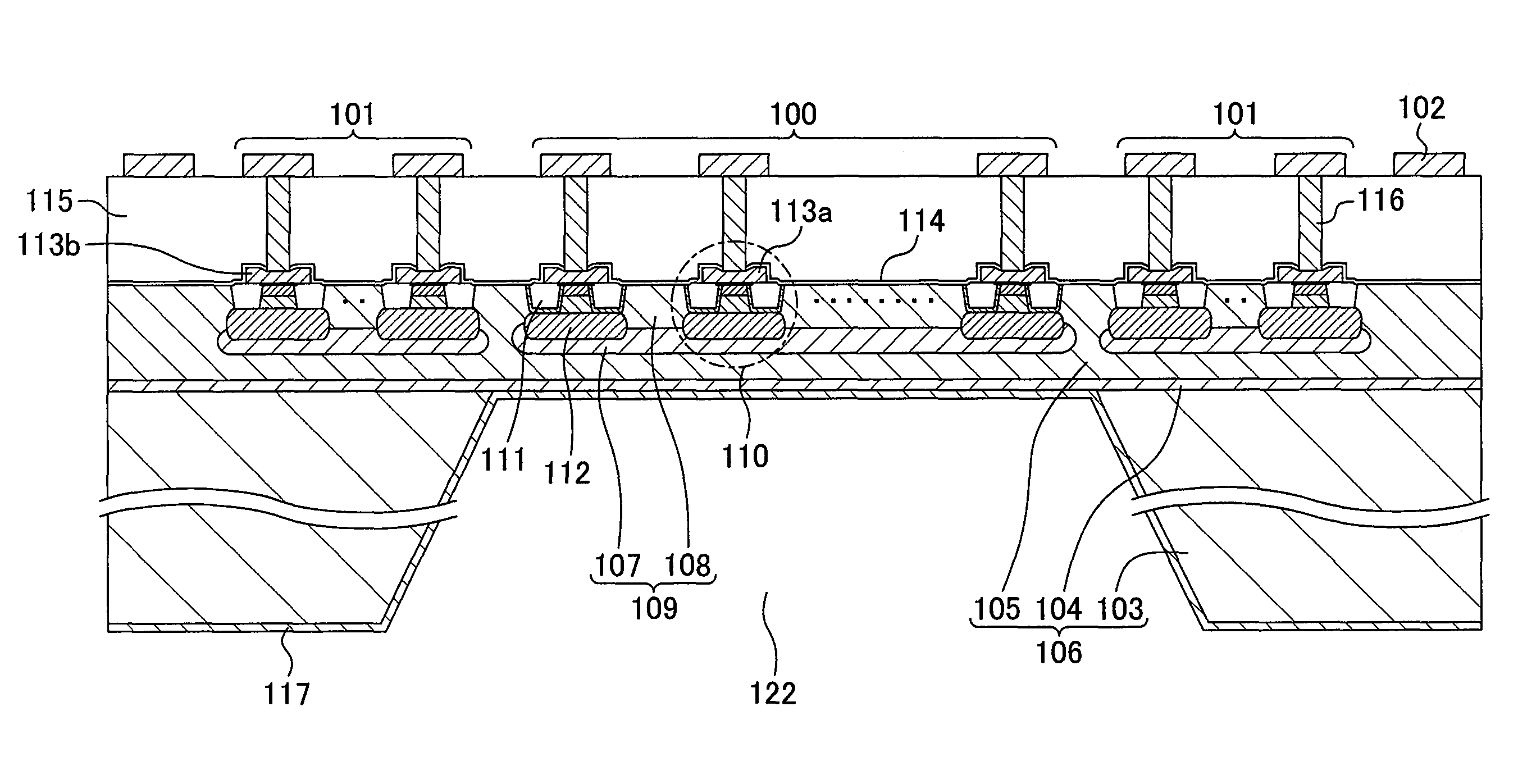
[0053]FIG. 3 is a sectional view showing an example of a structure of a solid-state imaging element in accordance with Embodiment 2. FIG. 3 shows a section of the same part as that taken along the line II-II in FIG. 1.
[0054]The solid-state imaging element of the present embodiment is a solid-state imaging element of Embodiment 1 which further includes a reflective film 117 on the reverse face of the layered substrate 106 for covering at least the recess 122. The reflective film 117 has a thickness of 1 μm or greater.
[0055]Preferably, the reflective film 117 is made of metal having a high reflectance, such as Au, Ag, Al or the like. Alternatively, the reflective film 117 may be made of a dielectric material or an organic material rather than metal having a high reflectance, which can attain the same effects as those in the present invention. The dielectric material includes SiO2, TiO2, and the like.
[0056]The reflective film 117 made of a metal material, a dielectric material, or an o...
embodiment 3
[0058]FIG. 4 is a sectional view showing an example of a structure of a solid-state imaging element in accordance with Embodiment 3. In the solid-state imaging element of the present embodiment, as shown in FIG. 4, the P+-type layer 104 at a high concentration is formed by ion implantation rather than epitaxial growth so as to form a peak point of the P-type impurity where the layered substrate 106 is thinned in the imaging region 100. Specifically, the peak point in the P+-type layer 104 under the PN photodiode 109 is located shallower than that in the P+-type layer 104 under the MOS transistors other than the PN photodiode 109 in the imaging region 100.
[0059]Since the P+-type layer 104 is used as an etching stopper in etching the reverse face portion of the substrate for forming the recess 122, the thickness of the layered substrate 106 in the MOS transistor formation region above the recess 122 where the layered substrate 106 is thinned can be set greater than that in the PN phot...
PUM
 Abstract
Description
Claims
Application Information
 - R&D
- Intellectual Property
- Life Sciences
- Materials
- Tech Scout
- Unparalleled Data Quality
- Higher Quality Content
- 60% Fewer Hallucinations
Browse by: Latest US Patents, China's latest patents, Technical Efficacy Thesaurus, Application Domain, Technology Topic, Popular Technical Reports.
© 2025 PatSnap. All rights reserved.Legal|Privacy policy|Modern Slavery Act Transparency Statement|Sitemap|About US| Contact US: help@patsnap.com