Semiconductor device and method for manufacturing same

a semiconductor and semiconductor technology, applied in semiconductor devices, semiconductor/solid-state device details, semiconductors, etc., can solve the problems of reducing the parasitic capacitance of the substrate, limiting the embedded insulating film to a silicon oxide film etc. having a higher heat resistance, and the conventional technique does not reduce the parasitic capacitance well with respect to the substrate. , the effect of suppressing the coupling capacitance and small thickness of the substra

Inactive Publication Date: 2010-07-06
NEC CORP
View PDF14 Cites 17 Cited by
  • Summary
  • Abstract
  • Description
  • Claims
  • Application Information

AI Technical Summary

Benefits of technology

[0036]In a preferred embodiment of the semiconductor device of the present invention, low-permittivity insulator rods including low-permittivity insulating film embedded in the semiconductor substrate underlying the inductor-forming region are disposed, and the substrate thickness is made small. This configuration is capable of suppressing the coupling capacitance between the inductor and the substrate to a lower value and also reducing the current induced in the substrate.
[0037]Moreover, if the inductor-forming region is provided with high-permeability material rods wherein a soft magnetic material is embedded within openings having a high aspect ratio, size reduction of the inductor can be achieved while suppressing the eddy current.
[0038]A configuration wherein a mixture of a soft magnetic material (high-permeability material) and a low-permittivity material is embedded within the openings in the inductor-forming area, if employed, achieves reduction in the capacitance between the lines of the inductor in addition to the size reduction of the inductor. This configuration reduces the loss and size of the RF circuit including the inductor, and achieves a semiconductor chip on which both a digital signal processing function and a RF circuit are mounted.
[0039]In the present invention, the semiconductor substrate is not limited to any specific one. By forming an area including low-permittivity insulator rods embedded in a silicon semiconductor substrate on which CMOS devices are formed, the silicon substrate, which is inherently a low resistance material, is provided with a high-resistance and low-permittivity area as a low-noise propagation area in a desired portion of the silicon substrate. The multi-layered interconnection structure includes an interconnection structure including two or more interconnect layers.BRIEF DESCRIPTION OF HE DRAWINGS
[0040]FIG. 1 is a sectional view of a semiconductor device according to a first embodiment of the present invention.
[0041]FIG. 2 is a sectional view of a semiconductor device according to a second embodiment of the present invention.

Problems solved by technology

All the conventional techniques are proposed for improving the performance of the inductors that are formed on the silicon substrate, and have respective problems as described hereinafter.
Although it is effective to embed an insulating film having a lower permittivity for reducing the parasitic capacitance, the low-permittivity insulating film cannot be used in the conventional techniques because a transistor-forming process is scheduled after embedding the insulating film.
Use of a structure, wherein the insulating film is embedded in the inductor-forming area before forming the transistors, inevitably limits the embedded insulating film to a silicon oxide film etc having a higher heat resistance.
Accordingly, the first conventional techniques do not well reduce the parasitic capacitance with respect to the substrate.
Since the silicon substrate is doped with impurities and thus has a low resistance, the substrate current cannot be well reduced so long as the substrate has a large thickness.
That is, it is impossible to well reduce the noise and loss therein.
In the case where the cross-sectional area / diameter of the ferromagnetic substance is larger compared to the embedded depth, there is an increased loss resulting from the eddy current caused by fluctuation of the magnetic field passing through the ferromagnetic substance area.
However, a smaller cross-sectional area employed alone is not expected to improve the magnetic flux density due to the resultant smaller covering area for the core region.

Method used


Image

  • Semiconductor device and method for manufacturing same
  • Semiconductor device and method for manufacturing same
  • Semiconductor device and method for manufacturing same

Examples


examples

[0130]Preferable examples of the present invention will be described in detail with reference to the drawings.

first example

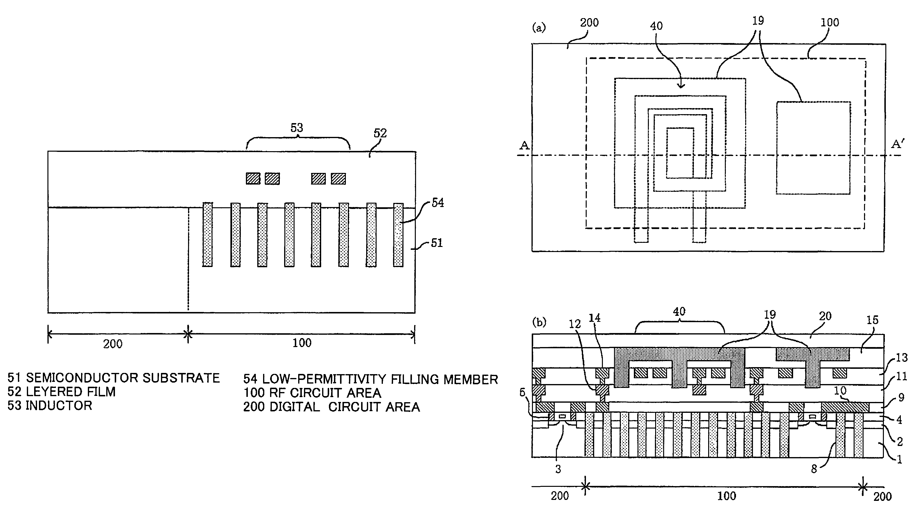
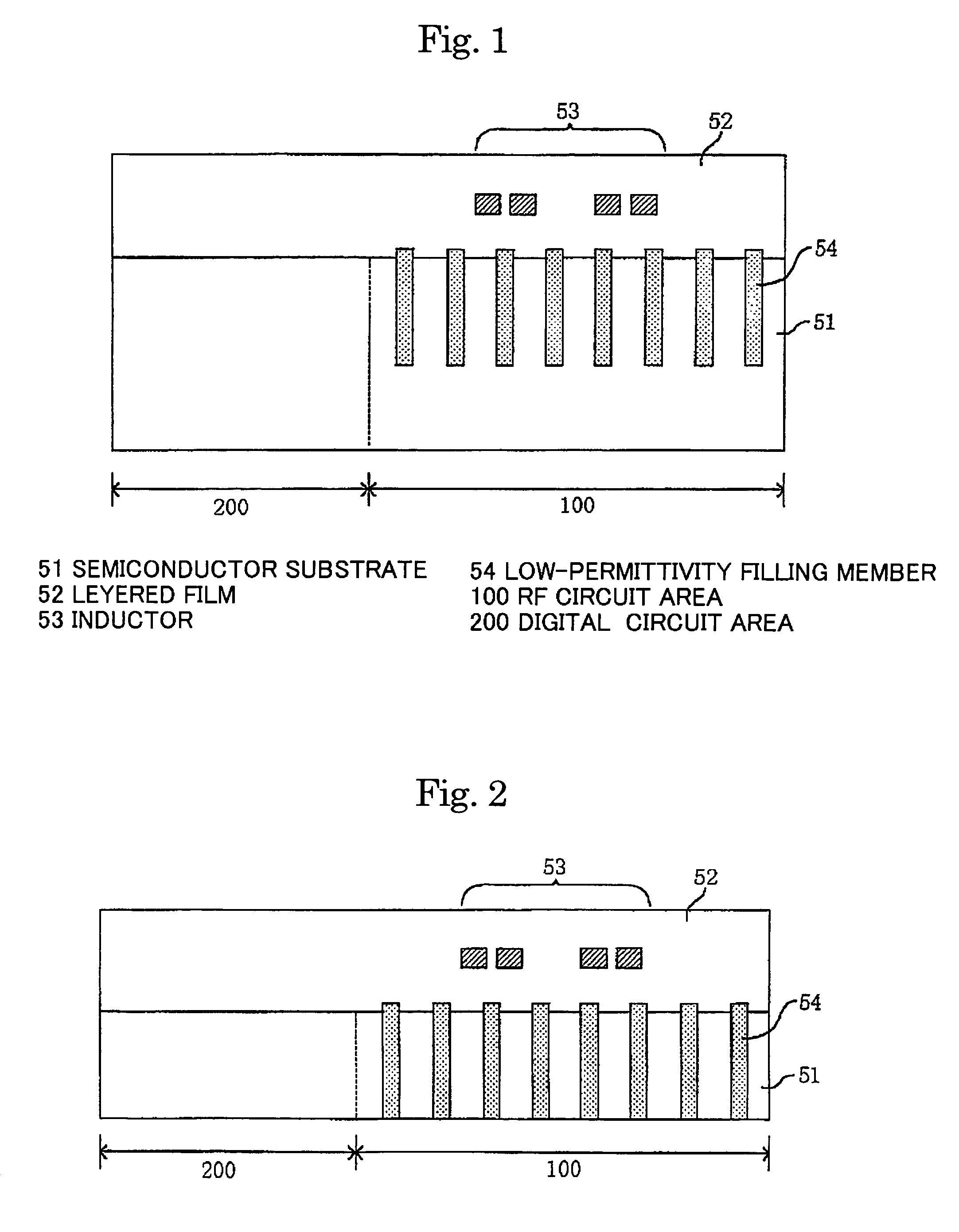
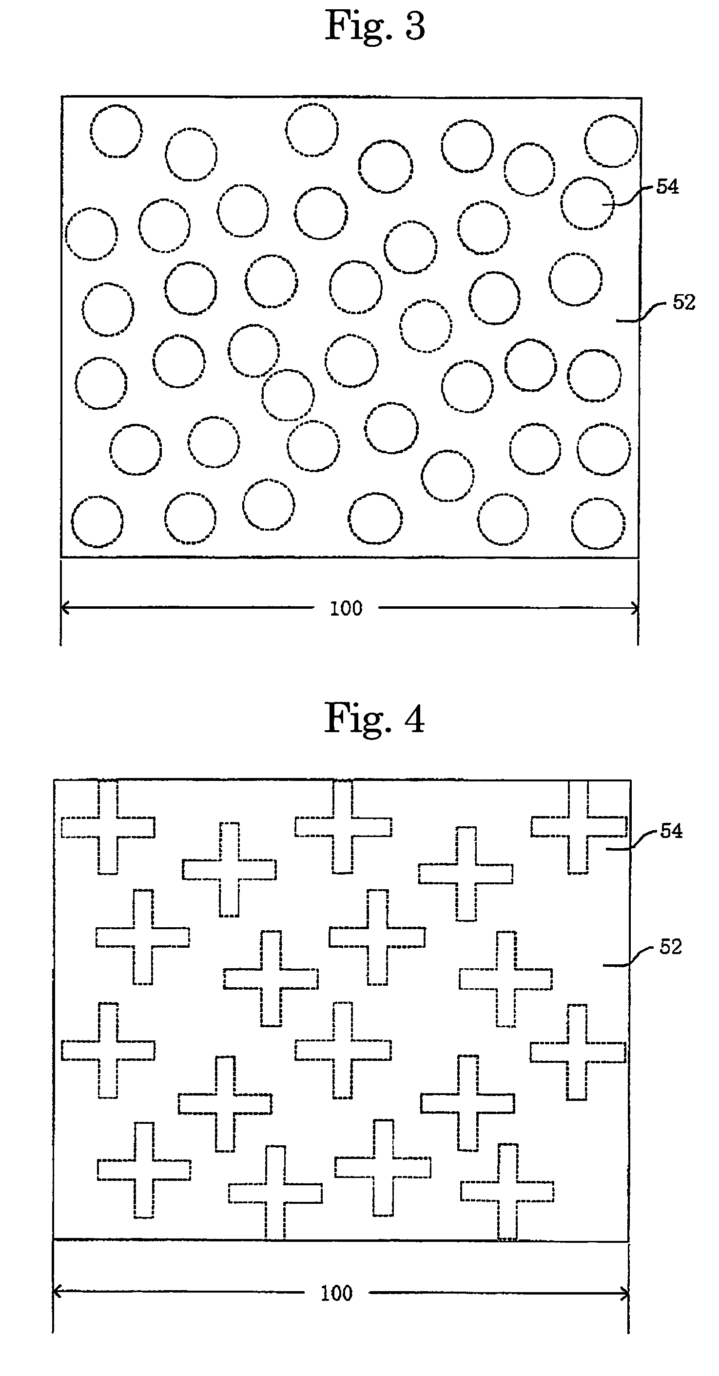
[0131]FIG. 8(a) is a top plan view showing the first example of the present invention, and FIG. 8(b) is a sectional view taken along line A-A′ in FIG. 8(a). On a silicon semiconductor substrate are provided an RF circuit area (high-frequency signal processing circuit area) 100 and a digital circuit area 200. MOSFETs 3 are formed in the regions isolated by shallow-trench-isolation film 2 on the silicon substrate 1, to configure CMOS circuits. In the silicon substrate of the RF circuit area 100 are located a plurality of low-permittivity insulator rods 8 in which low-permittivity insulator is embedded. In the present example, the low-permittivity insulator rods 8 penetrate the first interlevel dielectric film isolating the CMOS transistors and multi-layered interconnects to reach the internal of the silicon substrate. More specifically, the low-permittivity insulator rods are formed after all the CMOS transistor forming steps are finished; in other words, after all the high-temperatur...

second example

[0145]Referring to FIG. 19(a), the second example of the present invention is similar to the first example shown in FIG. 8 except that high-permeability isolation rods 21 without including a planar member are formed in the core of the inductor and the periphery thereof instead of the high-permeability isolation regions (19) each including a planar member and a rod and that the bottom surface of the low-permittivity insulating rods 8 is not exposed from the bottom surface of the substrate.

[0146]The fabrication method of the present example is similar to that of the first example in the steps up to the step shown in FIG. 15. Thereafter, the fifth interlevel dielectric film 15 is grown on the interconnect layers configuring the inductor 40, followed by forming openings penetrating the fifth interlevel dielectric film 15 and the fourth interlevel dielectric film 13 to reach the third interlevel dielectric film 11. The diameter of the openings is generally 1 μm to 2 μm, but not limited t...


PUM


Abstract

An object of the present invention is to mount both a RF circuit including an inductor formed therein and a digital circuit on a single chip.MOSFETs are formed on a semiconductor substrate 1 in regions isolated by an element isolation film 2. A plurality of low-permittivity insulator rods including a low-permittivity insulator embedded therein and penetrating a first interlevel dielectric film 4 to reach the internal of the silicon substrate are disposed in the RF circuit area 100. An inductor 40 is formed on the interlevel dielectric film in the RF circuit area by using multi-layered interconnects. A high-permeability isolation region in which a composite material including a mixture of high-permeability material and a low-permittivity material is formed in the region of the core of the inductor and periphery thereof.

Description

[0001]This application claims the benefit of International Patent Application No. PCT / JP2004 / 008450, filed Jun. 16, 2004, which claims priority of Japanese patent application No. 2003-170267.TECHNICAL FIELD[0002]The present invention relates to a semiconductor device capable of processing a high-frequency signal and a fabrication method thereof and, more particularly, to a semiconductor device including at least a high-frequency signal processing area on a semiconductor substrate and a fabrication method thereof.BACKGROUND ART[0003]Development of mobile computing requires a silicon chip to have a radio frequency communication function (RF communication function). A conventional silicon chip has therein CMOS gates including CMOS transistors, wherein signal processing is performed only in a digital logic processing scheme using the CMOS gates. On the other hand, the RF communication function is directed to analog signal processing, and includes an amplifying function for a received wa...

Claims


Application Information

Patent Timeline
Patent Type & Authority Patents(United States)
IPC IPC(8): H01L29/76H01L21/02H01L21/822H01L23/522H01L23/552H01L27/06H01L27/08H01L29/06
CPCH01L21/8221H01L23/5227H01L23/552H01L27/0617H01L27/0688H01L27/08H01L28/10H01L2924/0002H01L29/0657H01L2924/00H01L2924/00011H01L2224/80001
Inventor HAYASHI, YOSHIHIROINOUE, NAOYAHIJIOKA, KENICHIRO
Owner NEC CORP
Why Eureka
Try Eureka