High time-resolution ultrasensitive optical detector, using grating coupling

a technology of ultra-sensitive optical detectors and couplings, applied in the direction of photometry, photometry using electric radiation detectors, instruments, etc., can solve the problems of reducing overall efficiency, limited performance, and difficulty in reducing detection efficiency, etc., to achieve the effect of increasing detection efficiency and reducing the cost of operation

Inactive Publication Date: 2010-07-27
COMMISSARIAT A LENERGIE ATOMIQUE ET AUX ENERGIES ALTERNATIVES
View PDF11 Cites 12 Cited by
  • Summary
  • Abstract
  • Description
  • Claims
  • Application Information

AI Technical Summary

Benefits of technology

[0032]Operating at normal incidence makes it possible to consider simple positioning and reduced-space system in a cryostat, and the possibility of extending the coupling principle to a matrix of detectors used for example in imaging.
[0039]The structure of the optical detector, object of the invention, makes it possible to improve detection efficiency substantially using the one-dimensional dielectric grating located above the detecting element forming a serpentine.

Problems solved by technology

SSPDs potentially have all of the above-mentioned qualities and are good candidates to replace current avalanche photodiodes and photomultiplier tubes, whose performance is limited, especially in the infrared region.
The only way to increase this would be to increase the thickness of the NbN layer, but the relationship between the hot spot section and the section of the superconducting track would decrease, since the width of this track is limited to about 50 nm, and this would result in a drop in overall efficiency.
It would probably be difficult to considerably increase detection efficiency without changing the design of the optical coupling.
But, in fact, detection efficiency is limited by the great length of NbN.
In addition, the feasibility of monocrystalline NbN growth on the silicon has not yet been clearly demonstrated: the epitaxial growth of NbN on Si requires delicate surface treatments of the silicon as well as an examination of the deposit of interface layers by epitaxy.
However, neither the structuration of the waveguide and of the NbN in the plane of the layers, nor the practical carrying out of the detector are considered in this document [Wang 04]: no technological solution including the choice of materials, a method of fabrication and the methods for injecting the light in the considered is provided.

Method used


Image

  • High time-resolution ultrasensitive optical detector, using grating coupling
  • High time-resolution ultrasensitive optical detector, using grating coupling
  • High time-resolution ultrasensitive optical detector, using grating coupling

Examples


Embodiment Construction

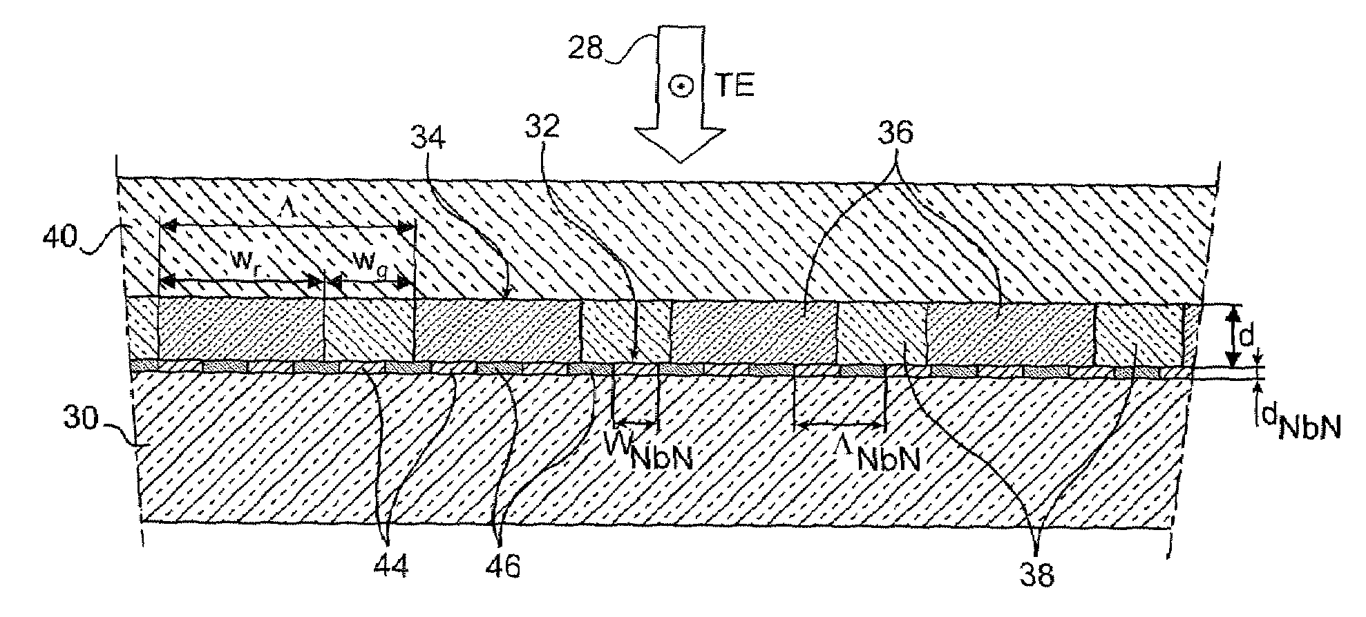
[0064]FIG. 4 is a schematic cross-section view of an example of the detector object of the invention. This detector is intended to detect an incident light 28, constituted of a single photon or of several photons.

[0065]The structure considered in FIG. 4 includes a dielectric substrate 30, whose refractive index is noted nO, and an ultra-thin superconducting layer 32, for example of NbN, whose thickness is equal to a few nanometers, on dielectric substrate 30. The latter is appropriate for the deposit of layer 32.

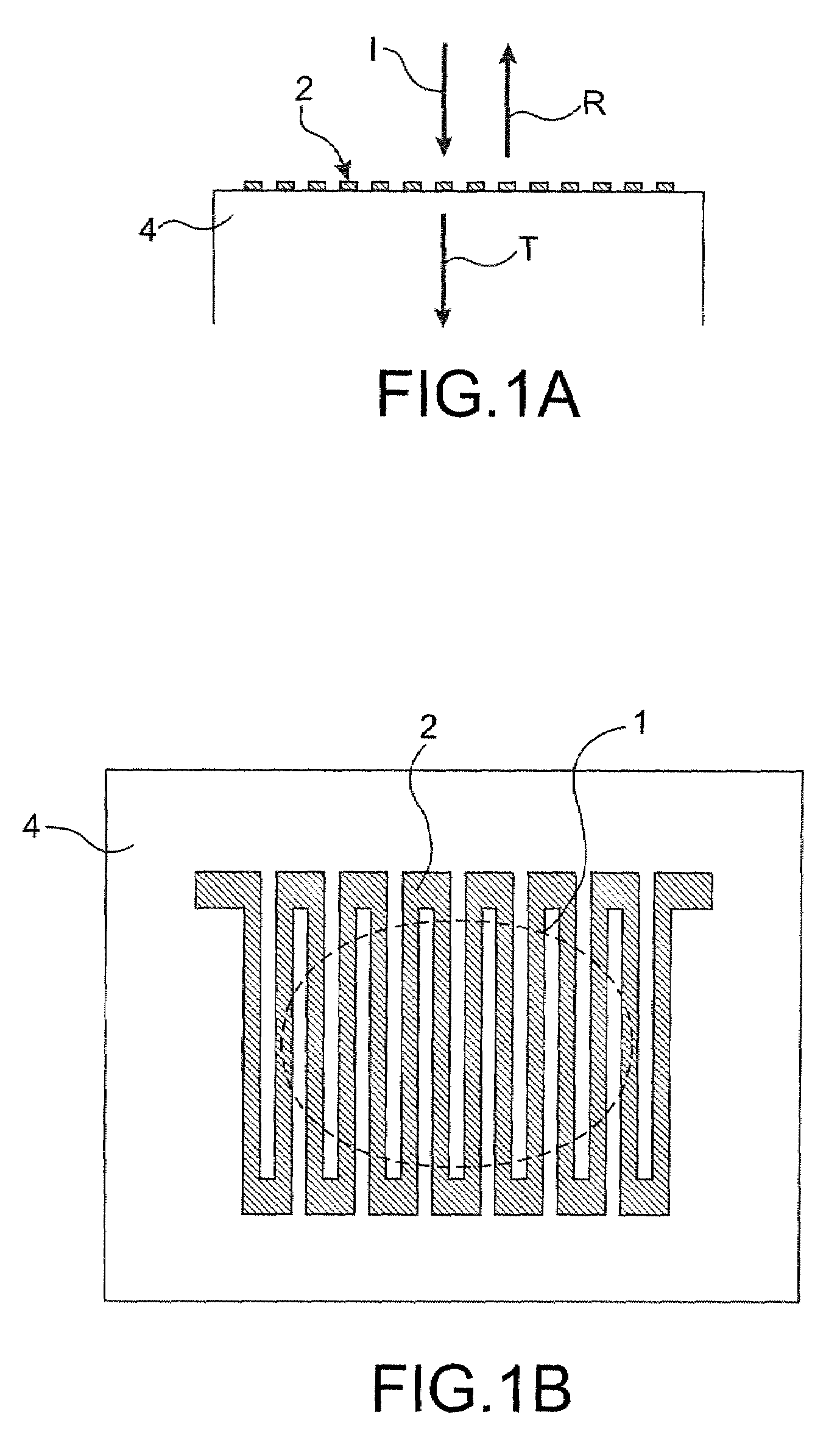
[0066]This layer 32 is intended to generate an electric signal using the energy of the photon(s) received. It forms a serpentine and therefore meanders as in prior art.

[0067]Reference will be made for example to FIG. 1B of the appended drawings where the layer includes parallel lines connected to one another by segments that are shorter than these lines and are perpendicular to the latter.

[0068]Other configurations can be considered for the serpentine, preferably configurati...


PUM


Abstract

This detector is intended to detect at least one photon and comprises a dielectric substrate (30), of index nO; a detecting element (32) forming a serpentine, placed on the substrate and generating a signal using the energy of the photon(s); a dielectric grating, formed of lines of index nH, alternating with lines of index nB, avec nH>nO and nH>nB, the grating being placed above the detecting element, the set grating-element presenting a resonant absorption in a given incidence and for a given polarisation; and a superstratum (40) having a refractive index ni, this superstratum being placed above the one-dimensional dielectric grating, nH being furthermore greater than ni.

Description

TECHNICAL FIELD[0001]This invention relates to a high time-resolution ultrasensitive optical detector, and in particular a superconducting single photon detector, more simply referred to as SSPD.[0002]The detector object of the invention uses a grating coupling and is able to operate at normal incidence.[0003]The invention is especially used to detect and locate the operating faults of a semiconductor integrated circuit, by detecting the emission of specific photons by defective transistors.[0004]It also applies to receiving and routing circuits for very high speed telecommunications, especially those that are intended for telecommunications satellites, because of the very low thermal dissipation of the detector object of the invention.[0005]The invention further applies to the coding and detecting of the quantum code key in a cryptographic system.[0006]It also applies to the fabrication of matrices of detectors for very highly sensitive imaging, as well as to single photon or corre...

Claims


Application Information

Patent Timeline
Patent Type & Authority Patents(United States)
IPC IPC(8): H01L39/00
CPCG01J1/02G01J1/0209G01J1/04G01J1/0407G01J1/42
Inventor FREY, LAURENT
Owner COMMISSARIAT A LENERGIE ATOMIQUE ET AUX ENERGIES ALTERNATIVES
Why Eureka
Try Eureka