Magneto-resistance effect element having diffusion blocking layer and thin-film magnetic head

a technology of diffusion blocking layer and magnetic head, which is applied in the field of magnetoresistance effect element and thin-film magnetic head, can solve the problems of extremely short life span, extremely difficult to form elements at a high dimensional accuracy, and loss of magneto-resistance effect element, etc., and achieve good element characteristics and high mr ratio

Inactive Publication Date: 2010-07-27
TDK CORPARATION
View PDF17 Cites 2 Cited by
  • Summary
  • Abstract
  • Description
  • Claims
  • Application Information

AI Technical Summary

Benefits of technology

[0014]It is an object of the present invention to provide a magnetoresistance effect element which is capable of achieving a high MR ratio and good element characteristics, and a thin-film magnetic head including such a magnetoresistance effect element.
[0022]With the above structure, since the semiconductor layer is included in the spacer layer, the resistance can be increased without a reduction in the MR ratio, so that the magnetoresistance effect element can produce a large output voltage with a low current density. The diffusion blocking layer included in the pinned layer is made of an oxide of an element whose electronegativity is equal to or smaller than Zn, e.g., ZnO, TaO, ZrO, MgO, TiO, or HfO, or is made of RuO. The diffusion blocking layer is capable of attracting and holding a substance, e.g., Mn, in a layer held in contact with the pinned layer for thereby preventing the substance from being diffused into the semiconductor layer in the spacer layer. As a result, the temperature at which the magnetoresistance effect element is heat-treated can be increased to achieve a good exchange coupling of the pinned layer, and at the same time a high MR ratio can be obtained by the action of the semiconductor layer in the spacer layer.
[0025]The pinned layer comprises an outer layer, a nonmagnetic intermediate layer held in contact with the outer layer, and an inner layer having a surface held in contact with the nonmagnetic intermediate layer and another surface held in contact with the spacer layer. The outer layer, the nonmagnetic intermediate layer, and the inner layer are successively stacked. The diffusion blocking layer may be provided as part of the outer layer. The diffusion blocking layer may be provided as part of the inner layer. For reliably blocking a substance, e.g., Mn, from being diffused from another layer into the semiconductor layer in the pinned layer, it is effective to place the diffusion blocking layer in the outer layer remote from the spacer layer, rather than in the inner layer close to the spacer layer. The diffusion blocking layer may be placed in both the inner layer and the outer layer.

Problems solved by technology

When the element is operated at the high current density, an electro-migration phenomenon occurs in which a metallic atom colliding with an electron migrates, and there is a fear that the magneto-resistance effect element will be destroyed by the migration of the atom and its life span becomes extremely short.
Further, when the element is operated at the high current density, an output noise caused by a spin transfer torque occurs, and a practical problem arises.
However, such a confined-current-path type magneto-resistance effect element has been difficult to manufacture, and it was extremely difficult to form the element at a high dimensional accuracy so as to be able to obtain desired performance.
However, though many materials may be used as the materials that makes up each layer of the spacer layer, specific materials that are best for increasing the MR ratio have not been proposed in the art.

Method used


Image

  • Magneto-resistance effect element having diffusion blocking layer and thin-film magnetic head
  • Magneto-resistance effect element having diffusion blocking layer and thin-film magnetic head
  • Magneto-resistance effect element having diffusion blocking layer and thin-film magnetic head

Examples


third embodiment

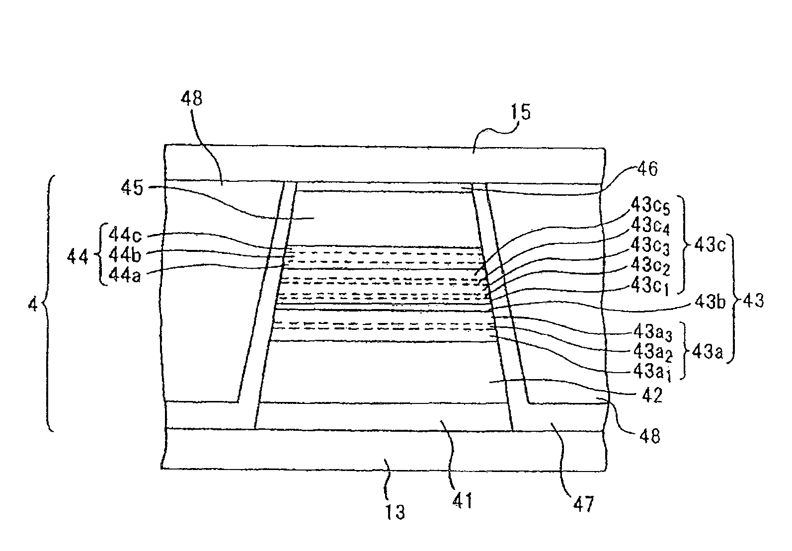
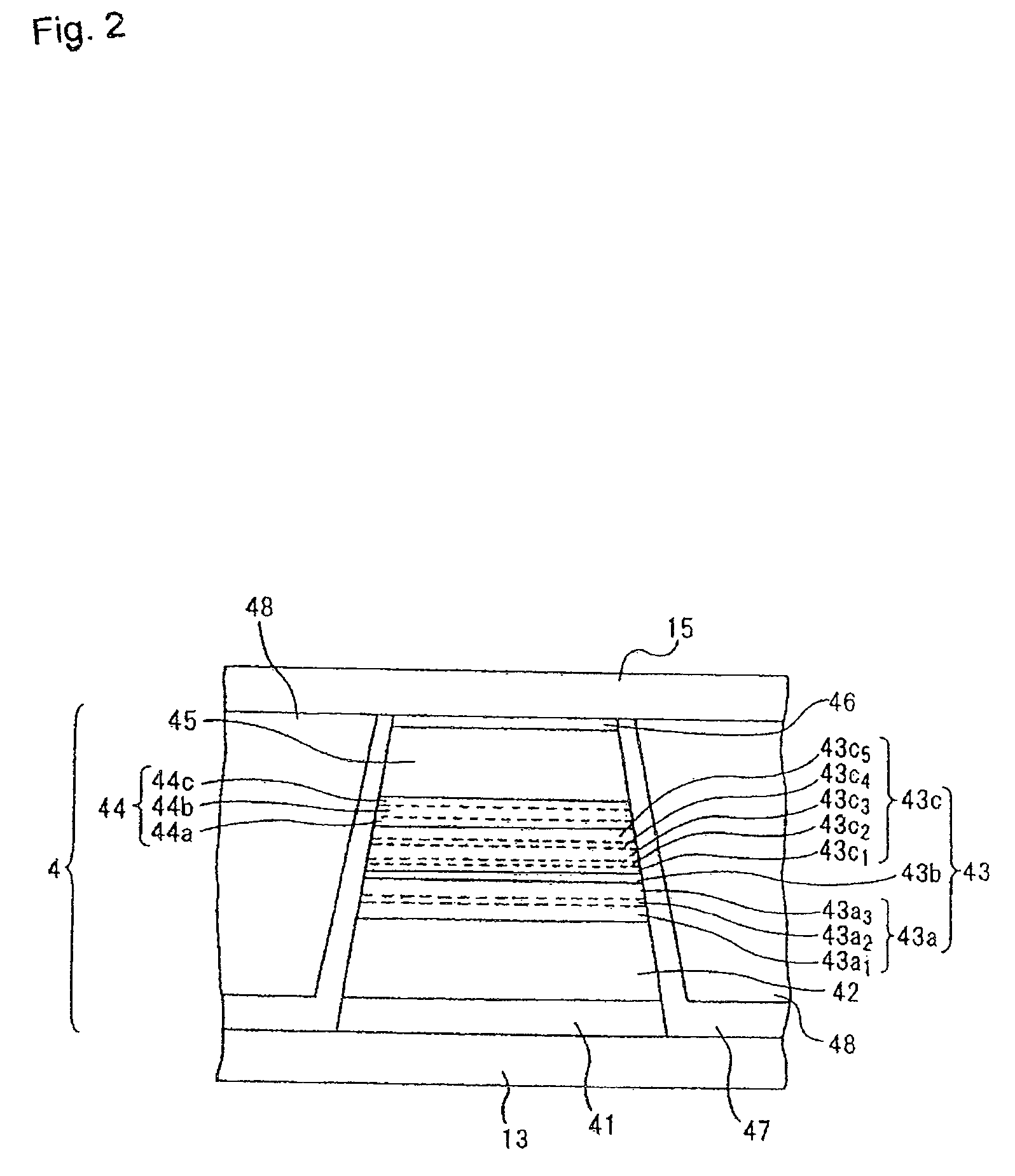
[0083]Although not shown, a structure may include ZnO film 43c2 provided as a diffusion blocking layer in inner layer 43c and ZnO film 43a2 provided as a diffusion blocking layer in outer layer 43a (see Table 1). These diffusion blocking layers are expected to further reduce the amount of Mn diffused into semiconductor layer 44b in spacer layer 44.

[0084]The thickness of ZnO film 43c2 in inner layer 43c and / or ZnO film 43a2 in outer layer 43 will be described below.

[0085]FIG. 8 shows a ZnO layer structure. According to the ZnO layer structure, at least one layer of Zn and one layer of 0 are required to provide ZnO. Since the interval between the layer of Zn and the layer of 0 is 0.195 nm, a film thickness of at least 0.195 nm is necessary for a ZnO film. Furthermore, in view of manufacturing process considerations, each of ZnO film 43a2 and ZnO film 43c2 should preferably have a thickness of at least 0.2 nm.

first embodiment

[0086]If the thickness of ZnO film 43c2 in inner layer 43c and / or ZnO film 43a2 in outer layer 43a increases, then the exchange coupling between pinned layer 43 and antiferromagnetic layer 42 tends to be broken. Specifically, as described above, ZnO films 43a2, 43c2 in pinned layer 43 are provided for the purpose of blocking the diffusion of Mn from antiferromagnetic layer 42, and do not contribute to the exchange coupling. If ZnO films 43a2, 43c2 which do not contribute to the exchange coupling are too thick, then the strength of the exchange coupling may possibly be reduced. FIG. 9 shows a magnetization curve of MR element 4. A magnetization curve of an MR element wherein no diffusion blocking layer is present in pinned layer 43 (ZnO: 0 nm) is regarded as representing an ordinary exchange coupling state. The MR element wherein ZnO film 43a2 is provided in outer layer 43a (ZnO: 0.6 nm) has a magnetization curve which is substantially the same as the magnetization curve representin...


PUM


Abstract

A magnetoresistance effect element (MR element) for use in a thin-film magnetic head has a buffer layer, an antiferromagnetic layer, a pinned layer, a spacer layer, a free layer, and a cap layer that are successively stacked. A sense current flows in a direction perpendicular to layer surfaces via a lower shield layer and an upper shield layer. The pinned layer comprises an outer layer having a fixed magnetization direction, a nonmagnetic intermediate layer, and an inner layer in the form of a ferromagnetic layer. The spacer layer comprises a first nonmagnetic metal layer, a semiconductor layer made of ZnO, and a second nonmagnetic metal layer. The inner layer or the outer layer includes a diffusion blocking layer made of an oxide of an element whose electronegativity is equal to or smaller than Zn, e.g., ZnO, TaO, ZrO, MgO, TiO, or HfO, or made of RuO.

Description

BACKGROUND OF THE INVENTION[0001]1. Field of the Invention[0002]The present invention relates to a magneto-resistance effect element and a thin-film magnetic head.[0003]2. Description of the Related Art[0004]Magnetic disk drives employ a thin-film magnetic head having a magneto-resistance effect element (MR element) for reading magnetic signals. In recent years, efforts have been made to design magnetic disk drives for higher recording densities, and accordingly there are growing demands for thin-film magnetic heads, particularly magneto-resistance effect elements, which satisfy higher-sensitivity and higher-output requirements.[0005]A CIP-GMR (Current in Plane—Giant Magnetoresistance) element which is a giant magneto-resistance effect element having a nonmagnetic layer between ferromagnetic layers and passing a sensing current in parallel to a layer surface, has been conventionally developed as a reproducing element in a thin-film magnetic head. On the other hand, a magnetic head t...

Claims


Application Information

Patent Timeline
Patent Type & Authority Patents(United States)
IPC IPC(8): G11B5/33
CPCB82Y25/00G01R33/093H01F10/3272H01F10/3259G11B5/3906Y10T428/1121
Inventor MIZUNO, TOMOHITOMACHITA, TAKAHIKOHIRATA, KEITSUCHIYA, YOSHIHIROHARA, SHINJI
Owner TDK CORPARATION
Why Eureka
Try Eureka