On die termination circuit and method for calibrating the same

a termination circuit and die technology, applied in logic circuit coupling/interface arrangement, pulse technique, instruments, etc., can solve problems such as noise and current consumption, signal reflectivity to be more critical, and general cause of impedance mismatch, so as to reduce noise and current consumption

Active Publication Date: 2010-08-24
SK HYNIX INC
View PDF27 Cites 21 Cited by
  • Summary
  • Abstract
  • Description
  • Claims
  • Application Information

AI Technical Summary

Benefits of technology

[0019]Embodiments of the present invention are directed to providing an ODT circuit that can reduce noise and current consumption caused by a direct use of a ZQ node voltage for generating a calibration code set.

Problems solved by technology

However, the reduction in the swing width of the signal has a great influence on an external noise, causing signal reflectivity to be more critical at an interface terminal due to impedance mismatch.
Such impedance mismatch is generally caused by an external noise, a variation of a power supply voltage, a change in an operating temperature, a change in a manufacturing process, etc.
The impedance mismatch may lead to a difficulty in high-speed data transmission and distortion of output data.
If semiconductor circuits receive the distorted output signal through an input terminal, problems such as a setup / hold failure and an error in decision of an input level may frequently arise.
However, the ODT circuits do not always have both the pull-up resistance unit and the pull-down resistance unit.
Therefore, it takes considerable time to stabilize the voltage of the ZQ pin.
However, in such a case, a resistance of 480Ω, including the external resistance of 240Ω and the calibration resistance of 240Ω, always exists between the source voltage VDDQ and the ground voltage VSSQ, which may significantly increase the current consumption.

Method used


Image

  • On die termination circuit and method for calibrating the same
  • On die termination circuit and method for calibrating the same
  • On die termination circuit and method for calibrating the same

Examples


Embodiment Construction

[0025]Hereinafter, an on die termination (ODT) circuit and a method for calibrating the ODT circuit in accordance with the present invention will be described in detail with reference to the accompanying drawings.

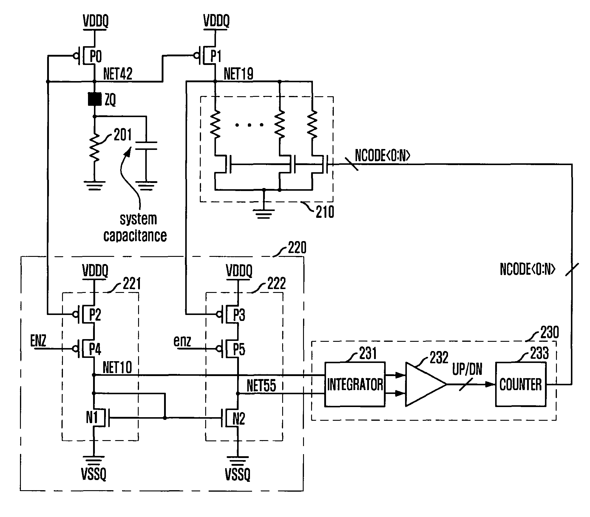
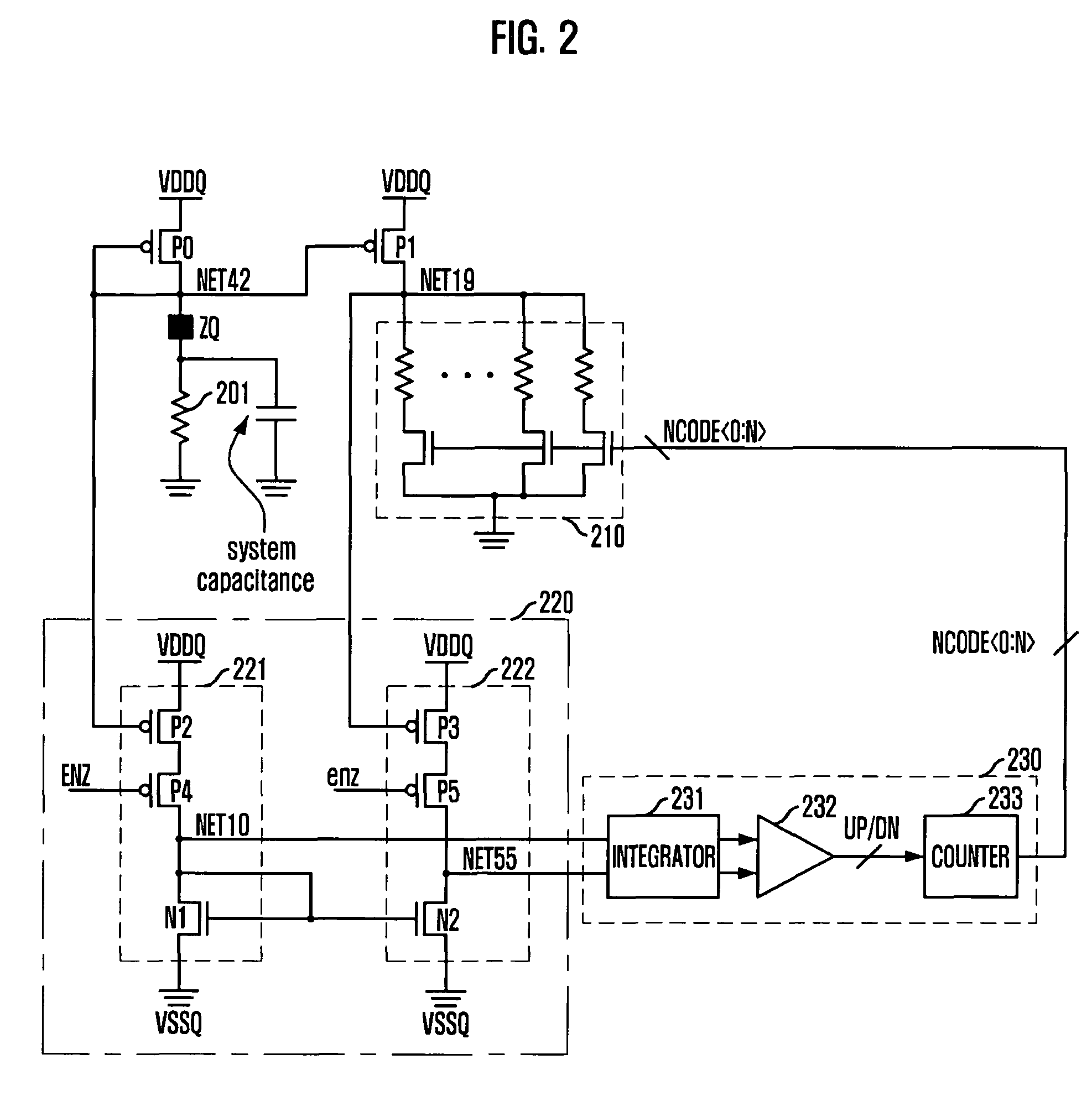
[0026]FIG. 2 is a circuit diagram of a calibration circuit of an ODT circuit for generating a calibration code set in accordance with an embodiment of the present invention.

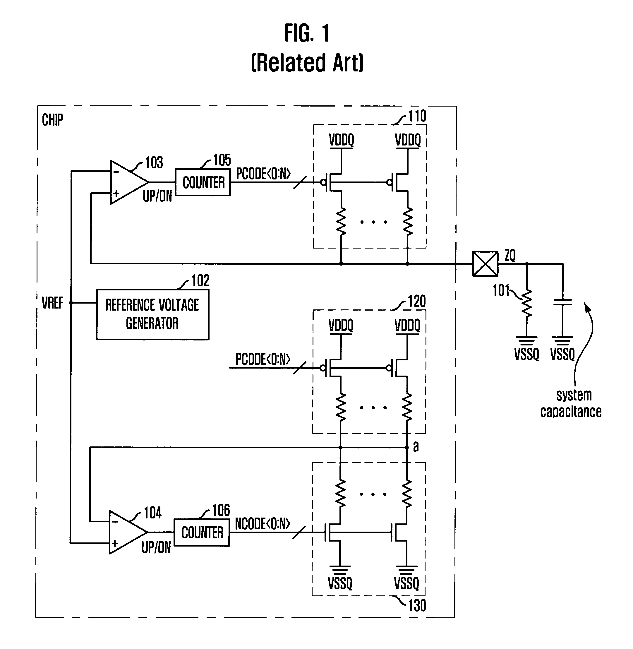
[0027]A calibration circuit of the ODT circuit for generating only one calibration code set is illustrated in FIG. 2. In some cases, an ODT circuit requires only one calibration code set. Even in other cases where two calibration code sets are required, a first calibration code set is primarily generated through a comparison with an external resistor, and then a second calibration code set is generated using the first calibration code set. Therefore, it is important to generate the first calibration code set using the external resistor connected to the ZQ pin (node).

[0028]Referring to FIG. 2, the ODT cir...


PUM


Abstract

On die termination circuit and method for calibrating the same includes a external resistor connected to a first node, a plurality of calibration resistors connected to a second node, the plurality of calibration resistors being turned on / off in response to a calibration code set, a current mirror configured to mirror currents of the first node and the second node and a code generator configured to generate a calibration code set according to the mirrored currents. In accordance with a method for calibrating an on die termination circuit of the present invention, the method includes a step of mirroring a current of a first node connected to an external resistor and a current of a second node connected to a plurality of calibration resistors and a step of generating a calibration code set according to the mirrored currents.

Description

CROSS-REFERENCE TO RELATED APPLICATIONS[0001]This application claims priority of Korean patent application number 10-2007-0046380, filed on May 14, 2007, which is incorporated by reference in its entirety.BACKGROUND OF THE INVENTION[0002]The subject matter relates to an on die termination (ODT) circuit used in a variety of semiconductor integrated circuits, and more particularly, to an ODT circuit with improved resolution.[0003]Semiconductor circuits are implemented into integrated circuit (IC) chips such as central processing units (CPUs), memories, and gate arrays, and are incorporated into a variety of electrical products such as personal computers, servers, and workstations. Most semiconductor circuits include an input circuit configured to receive signals from outside the circuit via input pads and an output circuit configured to provide internal signals to outside the circuit via output pads.[0004]As the operating speed of electrical products is increasing, a swing width of a ...

Claims


Application Information

Patent Timeline
Patent Type & Authority Patents(United States)
IPC IPC(8): H03K17/16H03K19/003
CPCG11C5/063G11C7/1051G11C7/1057H03K17/16H03K17/165H03K17/6871H04L25/0278H04L25/0298H03K17/6872H03K2217/0036H03K2217/94031G01R31/28
Inventor KOO, CHEUL-HEE
Owner SK HYNIX INC
Why Eureka
Try Eureka