Memory addressing controlled by PTE fields

a technology of page table entry and memory addressing, applied in the direction of memory addressing/allocation/relocation, instruments, computing, etc., can solve the problems of significantly reducing performance, time-consuming and laborious, and the process of activating a row of data within a dram device takes time. achieve the effect of reducing bank conflicts and access memory hot spots

Active Publication Date: 2010-09-28
NVIDIA CORP
View PDF6 Cites 407 Cited by
  • Summary
  • Abstract
  • Description
  • Claims
  • Application Information

AI Technical Summary

Benefits of technology

[0012]One advantage of the disclosed method is that the data kind bits may be used to guide and optimize the mapping process from a linear physical address space to a DRAM physical address space that is used to directly access one or more DRAM. The modified mapping process enables bank conflicts and access memory hot spots to be reduced when data is being accessed within the one or more DRAM.

Problems solved by technology

Because the memory is off-chip, the access speed associated with the memory is inherently slower than accessing or processing on-chip data, thereby creating a performance bottleneck.
The process of activating a row of data within a DRAM device takes time and incurs overhead.
However, if sequential requests access different rows within the same bank, then the activate operations become serialized, resulting in significantly diminished performance.
When the interleaving strategies described above are combined with the block-linear organization of a 2D surface within the DRAM devices, access “hot spots” naturally develop, whereby a disproportionate number of requests to the same bank within a given DRAM device are generated, leading to an increase in bank conflicts.
Further, access hot spots can concentrate access requests within a reduced set of DRAM devices, undermining the efficiency of DRAM device interleaving (also referred to as “data interleaving”).
These combined effects negatively impact overall system performance.
While the kind of data and size of the 2D surface determine the vertical alignment of banks and potential layout within the surface, there is really no efficient way for the graphics processing unit to exploit this information in order to avoid the performance degradation associated with memory access hot spots and bank conflicts.

Method used


Image

  • Memory addressing controlled by PTE fields
  • Memory addressing controlled by PTE fields
  • Memory addressing controlled by PTE fields

Examples


Embodiment Construction

[0021]In the following description, numerous specific details are set forth to provide a more thorough understanding of the present invention. However, it will be apparent to one of skill in the art that the present invention may be practiced without one or more of these specific details. In other instances, well-known features have not been described in order to avoid obscuring the present invention.

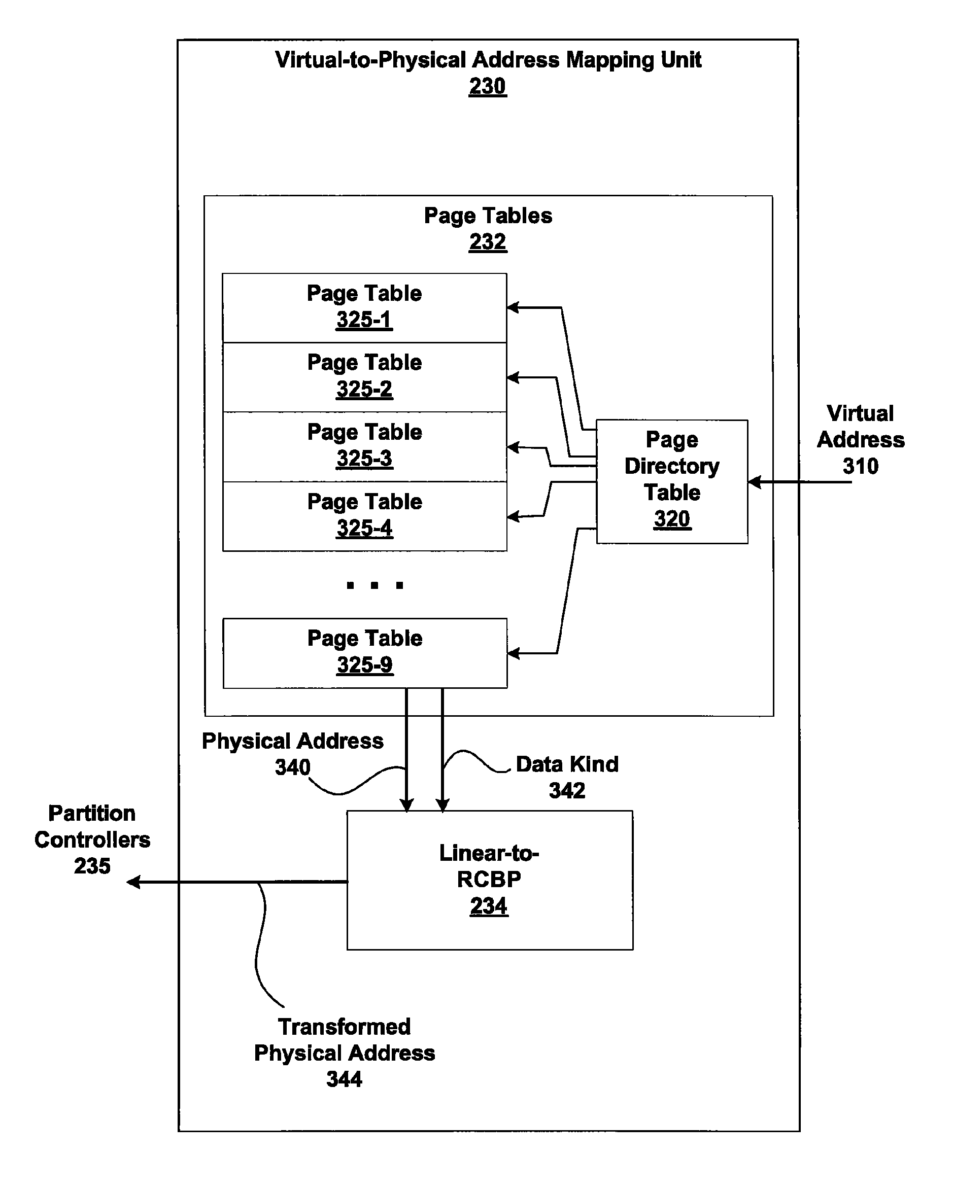
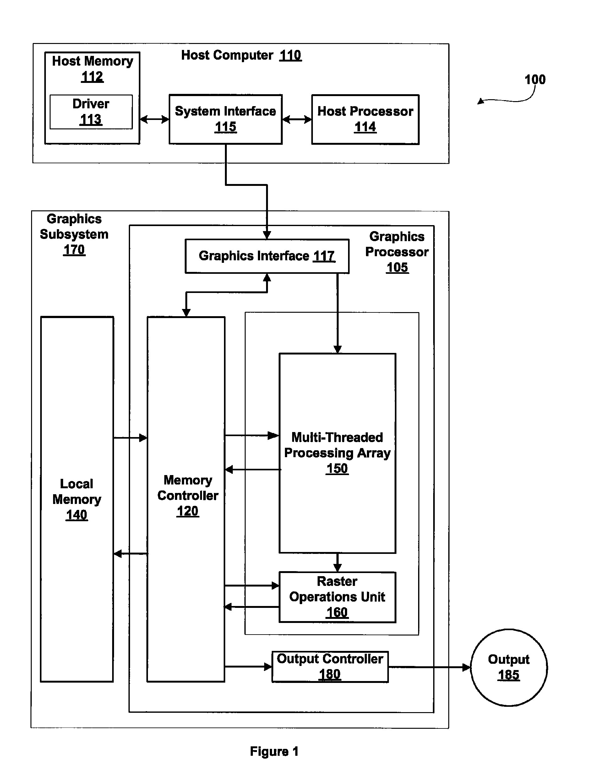
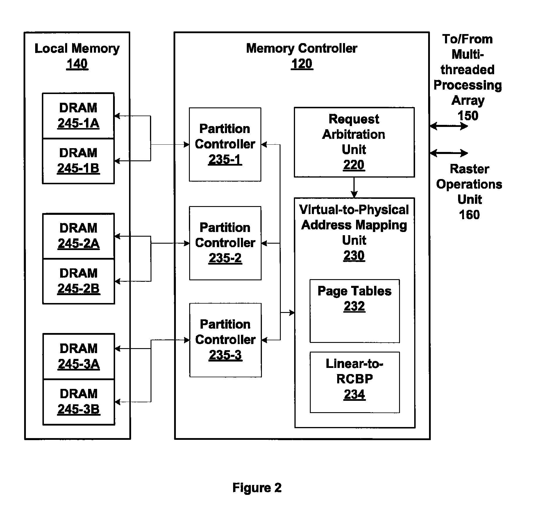
[0022]FIG. 1 illustrates a computing system 100 including a host computer 110 and a graphics subsystem 170, in accordance with one or more aspects of the present invention. Computing system 100 may be a desktop computer, server, laptop computer, personal digital assistant (PDA), palm-sized computer, tablet computer, game console, cellular telephone, computer-based simulator, or the like. The host computer 110 includes a host processor 114, a host memory 112, and a system interface 115. The system interface 115 may be an I / O (input / output) interface or a bridge device including a system ...


PUM


Abstract

Embodiments of the present invention enable virtual-to-physical memory address translation using optimized bank and partition interleave patterns to improve memory bandwidth by distributing data accesses over multiple banks and multiple partitions. Each virtual page has a corresponding page table entry that specifies the physical address of the virtual page in linear physical address space. The page table entry also includes a data kind field that is used to guide and optimize the mapping process from the linear physical address space to the DRAM physical address space, which is used to directly access one or more DRAM. The DRAM physical address space includes a row, bank and column address. The data kind field is also used to optimize the starting partition number and partition interleave pattern that defines the organization of the selected physical page of memory within the DRAM memory system.

Description

BACKGROUND OF THE INVENTION[0001]1. Field of the Invention[0002]Embodiments of the present invention generally relate to mapping virtual memory pages to physical memory pages in a local memory system based on dynamic random access memory and, more specifically, to memory addressing controlled by page table entry fields.[0003]2. Description of the Related Art[0004]Conventional graphics processing units use off-chip memory to store different kinds of data, such as image data and texture map data. Because the memory is off-chip, the access speed associated with the memory is inherently slower than accessing or processing on-chip data, thereby creating a performance bottleneck. The data stored within the external memory is used to generate and display sequential frames of graphics images and any input / output bottlenecks associated with accessing the external memory therefore impacts the overall performance of the graphics processing unit. The off-chip memory is typically constructed usi...

Claims


Application Information

Patent Timeline
Patent Type & Authority Patents(United States)
IPC IPC(8): G06F9/34G06F12/00
CPCG06F12/0607G06F12/10
Inventor VAN DYKE, JAMES M.EDMONDSON, JOHN H.
Owner NVIDIA CORP
Why Eureka
Try Eureka