Method and system for improved nickel silicide

a technology of nickel silicide and nickel silicide, applied in the field of nickel silicide, can solve the problems of high-performance logic that requires faster operation speed, problems may arise during the silicidation process, etc., and achieve the effects of reducing sheet resistance, reducing pipe defects, and improving mosfet performan

Active Publication Date: 2010-11-02
TEXAS INSTR INC
View PDF5 Cites 5 Cited by
  • Summary
  • Abstract
  • Description
  • Claims
  • Application Information

AI Technical Summary

Benefits of technology

[0005]Embodiments of the invention provide a number of technical advantages. Embodiments of the invention may include all, some, or none of these advantages. According to one embodiment, MOSFET performance is improved by a method of nickel silicidation that lowers sheet resistance and reduces pipe defects without increasing the thickness of the deposited nickel layer. In one embodiment, such advantages are achieved by amorphizing the silicon in the source and drain regions with a heavy ion. This amorphization method may be simple, effective, inexpensive, and CMOS compatible.

Problems solved by technology

In addition, use of the devices in, for example, high performance logic requires faster operational speed.
However, because of the diffusion characteristics of nickel, problems may arise during the silicidation process, such as pipe defects.

Method used


Image

  • Method and system for improved nickel silicide
  • Method and system for improved nickel silicide

Examples


Embodiment Construction

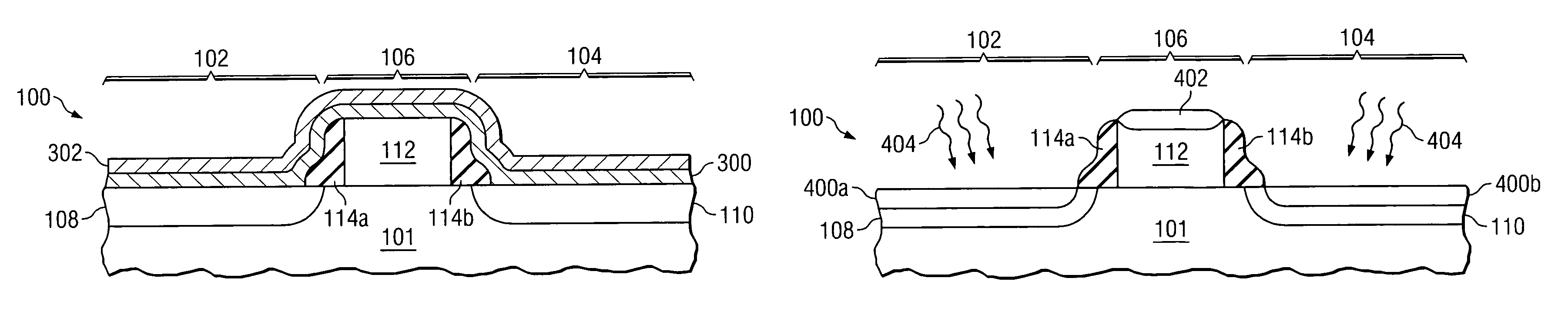
[0009]Example embodiments of the present invention and their advantages are best understood by referring now to FIGS. 1 through 4 of the drawings, in which like numerals refer to like parts.

[0010]FIG. 1 is a cross-sectional view illustrating a portion of a metal-oxide semiconductor field effect transistor (“MOSFET”) 100 in accordance with one embodiment of the present invention. MOSFET 100, as used throughout this detailed description, represents a partially completed MOSFET, such as an NMOS, PMOS, CMOS, or other suitable semiconductor device. In the illustrated embodiment, MOSFET 100 includes a substrate 101, a source region 102 having a source 108, a drain region 104 having a drain 110, and a gate region 106 having a gate 112.

[0011]Substrate 101 may be formed from any suitable semiconductor material, such as silicon. For example, substrate 101 may be a silicon wafer, a silicon wafer with previously embedded devices, an epitaxial layer grown on a wafer, a semiconductor on insulatio...


PUM

PropertyMeasurementUnit
temperatureaaaaaaaaaa

Abstract

According to one embodiment of the invention, a method for nickel silicidation includes providing a substrate having a source region, a gate region, and a drain region, forming a source in the source region and a drain in the drain region, annealing the source and the drain, implanting, after the annealing the source and the drain, a heavy ion in the source region and the drain region, depositing a nickel layer in each of the source and drain regions, and heating the substrate to form a nickel silicide region in each of the source and drain regions by heating the substrate.

Description

TECHNICAL FIELD OF THE INVENTION[0001]The present invention relates generally to the field of semiconductor devices and, more particularly, to a method and system for nickel silicide.BACKGROUND OF THE INVENTION[0002]Modern electronic equipment, such as televisions, radios, cell phones, and computers are generally constructed of solid state devices. Solid state devices include transistors, capacitors, resistors and the like. One type of transistor is a metal oxide semiconductor field effect transistor (MOSFET), such as NMOS, PMOS, or CMOS transistors. MOSFETs may be used in a myriad of electronic devices.[0003]Increasingly, MOSFETs are made smaller to reduce the size and increase performance of electronic equipment. In addition, use of the devices in, for example, high performance logic requires faster operational speed. One way to achieve faster operational speed is to reduce the series resistance of the source, drain, and gate regions. This has been accomplished using metal silicid...

Claims


Application Information

Patent Timeline
Patent Type & Authority Patents(United States)
IPC IPC(8): H01L21/44H01L21/477
CPCH01L21/28518H01L29/665H01L29/78H01L21/823807H01L21/823835
Inventor JAIN, AMITABHCHEN, PEIJUNKITTL, JORGE A.
Owner TEXAS INSTR INC
Why Eureka
Try Eureka