Polyoxometallates in memory devices

a technology of polyxometallates and memory devices, applied in semiconductor devices, digital storage, instruments, etc., can solve the problems of saturation of erasing characteristics, large leakage currents, and many technological obstacles, and achieve the effect of improving the situation and advantageous use of multi-bit storage devices

Inactive Publication Date: 2010-11-09
COMMISSARIAT A LENERGIE ATOMIQUE ET AUX ENERGIES ALTERNATIVES
View PDF8 Cites 14 Cited by
  • Summary
  • Abstract
  • Description
  • Claims
  • Application Information

AI Technical Summary

Benefits of technology

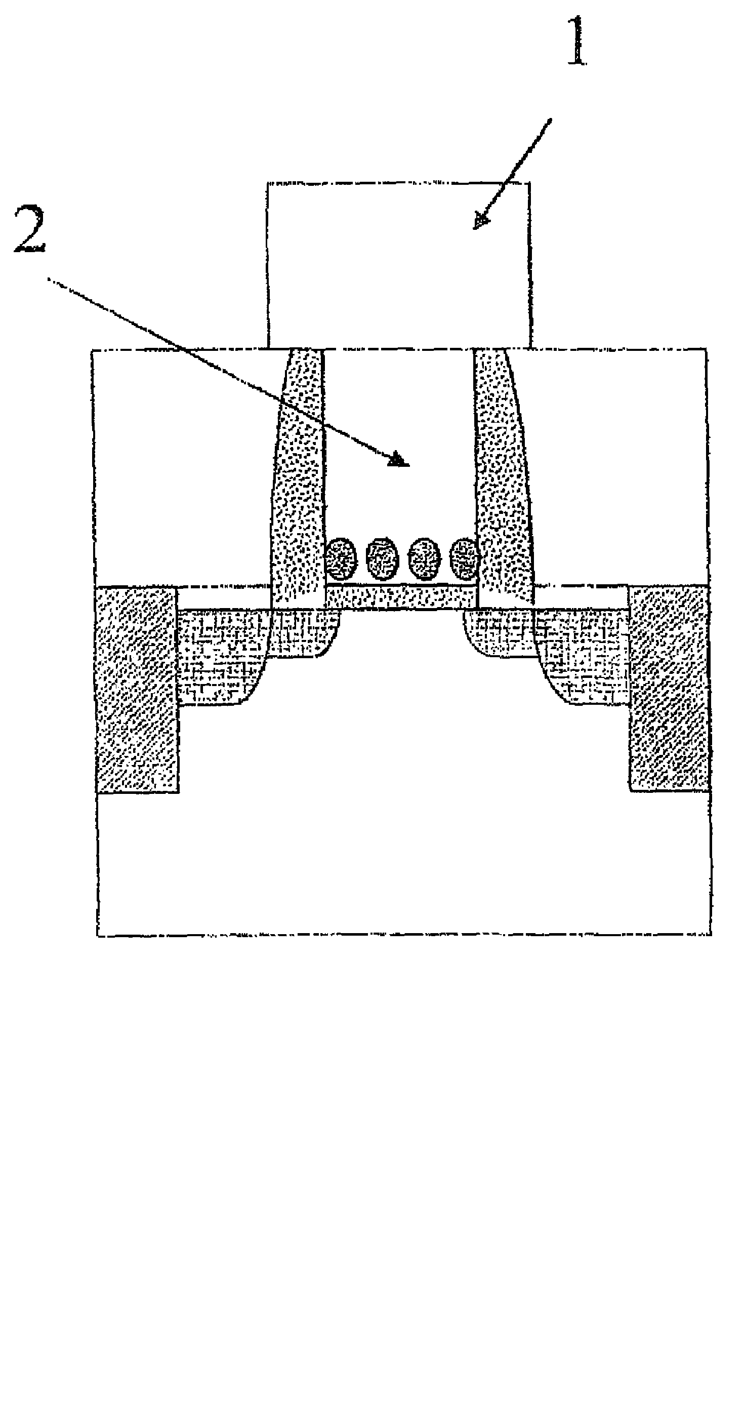
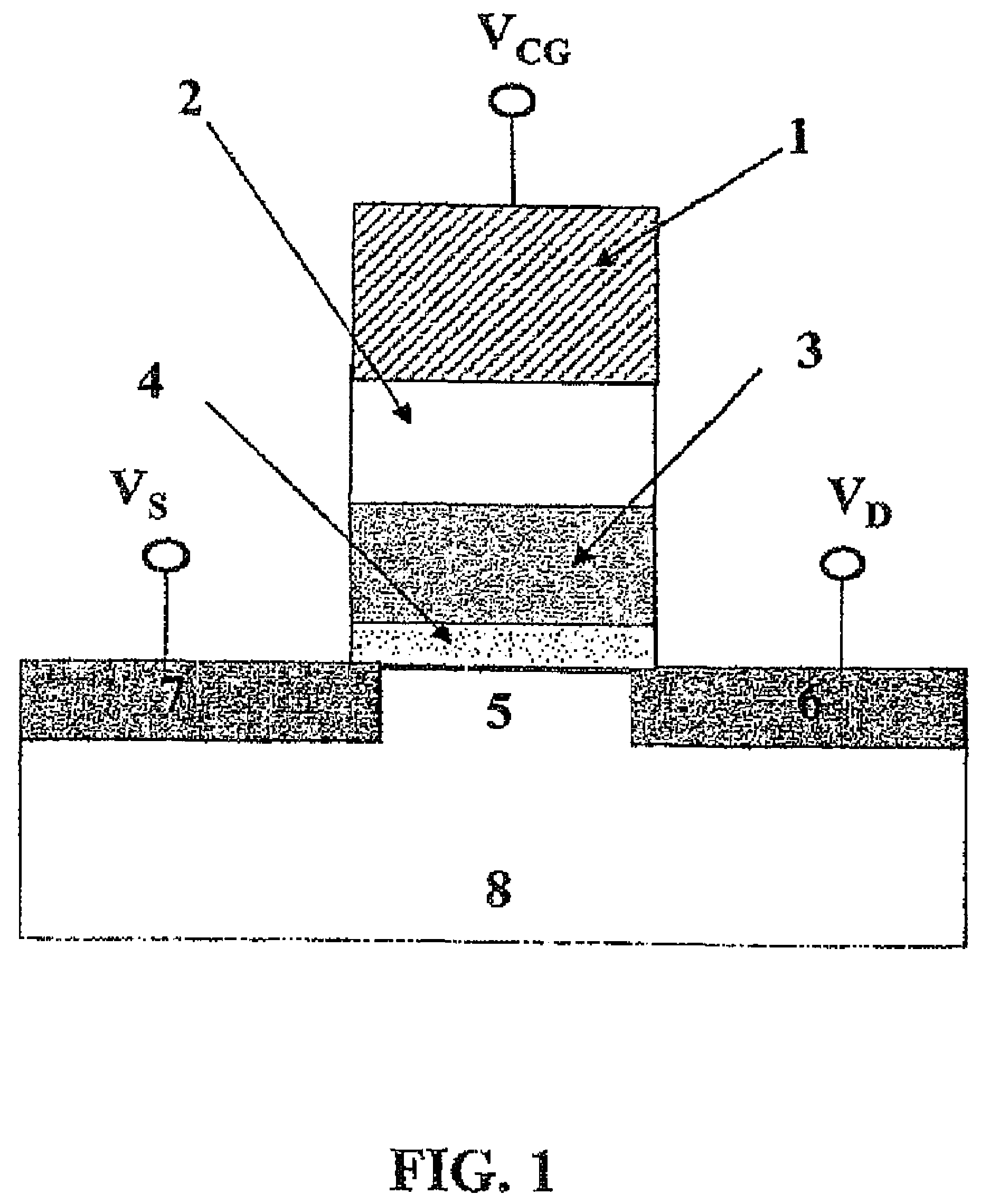
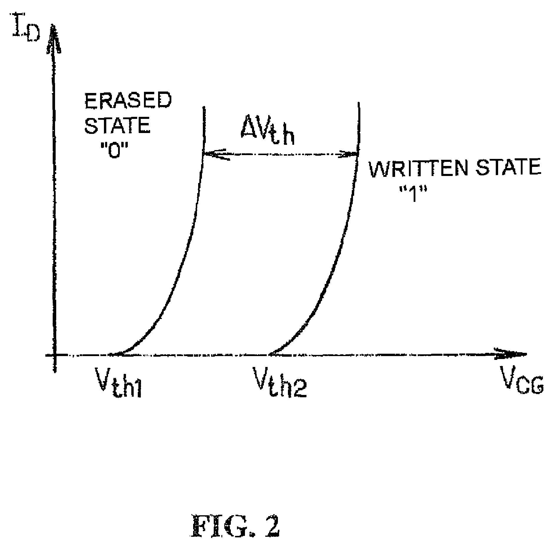
[0033]The present invention aims to improve the situation. It provides, for this purpose, a memory device comprising molecules capable of storing charges which are used for storing information. The expressions “charge storage molecules” and “molecules capable of storing charges” are used interchangeably in the present application. At least some of these molecules are and / or comprise at least one polyoxometallate (POM). The charge storage molecules have a multiplicity of oxidation states, enabling their advantageous use in multibit storage devices. The expression “multibit storage” denotes the storage of several bits in a memory cell.

Problems solved by technology

However, several technological obstacles oppose the ever-increasing miniaturization of memory devices.
However, to reduce the thickness of the tunnel oxide, in particular to below 8 nm, causes larger leakage currents.
However, the injection of electrons into the nitride layer by the control gate during the erasing phase leads to a saturation of the erasing characteristics (M. Sadd et al, IEEE Non-volatile Semiconductor Memory Workshop 2003, p.
However, such memory is obtained by complex processes which limit the future miniaturization thereof.
These compounds have very different structures and their homogeneous distribution within the SAxs is difficult to control.
Furthermore, the immobilization on a surface of a semiconductor or of the oxide by a SAM process is itself long, expensive and remains not very reproducible in terms of thickness and homogeneity of the layers.
The devices described do not make it possible to directly produce variations in the amounts of charge sufficient to obtain an electrical memory effect that can be used in DRAM and flash memory applications.
One of the main problems presented by the memory cells of the prior art is that they use organic compounds which are unstable, especially at high temperatures.
Specifically, it will be recalled that the organic compounds used in the memory cells of the prior art and which have redox properties are thermally unstable.
The thermal instability which characterizes the organic compounds of the prior art poses a serious problem during the design of multibit storage memory cells.

Method used


Image

  • Polyoxometallates in memory devices
  • Polyoxometallates in memory devices
  • Polyoxometallates in memory devices

Examples


example 2

Thermal Stability of the POMs

[0118]The thermal stability varies as a function of the structure and of the nature of the associated counter-ions. For example, the compound H3PMo12O40 decomposes at 443° C. and its potassium salt at 493° C. The diallyl-ammonium salts of POM, especially including PMo12O403−, are capable of withstanding temperatures above 300° C. in an ambient atmosphere (R. Baur et al., Chem. Abstr., 1993, 120: 334828). Also, the POx corresponding to the formula H3PMo12O40 is capable of withstanding temperatures ranging from −50 to 500° C. (H. Schmidtpott et al., Chem., Abstr, 1987, 106: 55168).

example 3

POM Gel

[0119]One charge storage molecule according to the invention is α2-[P2W17O61{(RSi)2O}]6− with α2-[P2W17O61]6− denoting a Dawson vacancy POM and R being a group comprising a function that enables the polymerization of vinyl type R=CH2═C(Me)C(O)OPr described by C. Mayer and R. Thouvenot (Chem. Mat., 2000, 12: 257).

[0120]According to another process described by S. Bareyt, et al., (JACS, 2005, 127: 6788), one molecule according to the invention is α2-[P2W17O61{SnCH2CH═CH2}]7−.

example 4

Charge Storage Molecule Comprising a Bond for Forming Self-Assembled Monolayers

[0121]According to a process similar to the preceding one, the molecule is α2-[P2W17O61{Sn(CH2)2CO2}]7−, the carboxylic groups enable the attachment onto any surface comprising groups capable of coupling with them such as hydroxyls.


PUM


Abstract

The invention relates to a DRAM memory device with a capacity associated with a field effect transistor, in which all or some of the molecules capable of storing the loads comprising a polyoxometallate are incorporated into the capacity, or a flash-type memory using at least one field effect transistor, in which the molecules capable of storing the loads comprising a polyoxometallate are incorporated into the floating grid of the transistor. The invention also relates to a method for producing on such device and to an electronic appliance comprising one such memory device.

Description

CROSS-REFERENCE TO RELATED APPLICATIONS[0001]This application is a U.S. national stage filing of International Patent Application No. PCT / FR2006 / 001882 filed on Aug. 2, 2006, which claims priority under the Paris Convention to French Patent Application No. 05 08263, filed on Aug. 8, 2005.FIELD OF THE DISCLOSURE[0002]The present invention relates to a charge storage memory device, its fabricating process and its use in the field of electronics.BACKGROUND OF THE DISCLOSURE[0003]Memory devices are present in all electronic systems for storing data. The base components which form them, the memory cells, are still the subject of intense research to improve their performance (retention, reliability, programming speed) especially by means of so-called innovative memory. The term “innovative” is understood to mean that they use storage mechanisms that until now have not been exploited in the field of electronics or else that they are novel in their architectures.[0004]In the design of nonvo...

Claims


Application Information

Patent Timeline
Patent Type & Authority Patents(United States)
IPC IPC(8): H01L27/108H01L21/8242
CPCB82Y10/00G11C11/56G11C13/0009G11C13/02H01L21/28273H01L29/42332H01L29/513H01L29/7881H01L29/792H01L51/0595G11C2213/53H01L29/40114H10K10/701
Inventor BIDAN, GERARDJALAGUIER, ERIC
Owner COMMISSARIAT A LENERGIE ATOMIQUE ET AUX ENERGIES ALTERNATIVES
Why Eureka
Try Eureka