
Electron beam apparatus and an aberration correction optical apparatus

lectron beam technology, applied in the direction of instruments, magnetic discharge control, beam deviation/focusing by electric/magnetic means, etc., can solve the adversely increased off-axis aberration of the entire optical system including an aberration correction optical apparatus, and the focus is significantly blurred, so as to achieve the same resolution, improve the effect of resolution and improve the beam transmission ra

Active Publication Date: 2011-01-04
EBARA CORP
View PDF67 Cites 8 Cited by
  • Summary
  • Abstract
  • Description
  • Claims
  • Application Information

AI Technical Summary

Benefits of technology

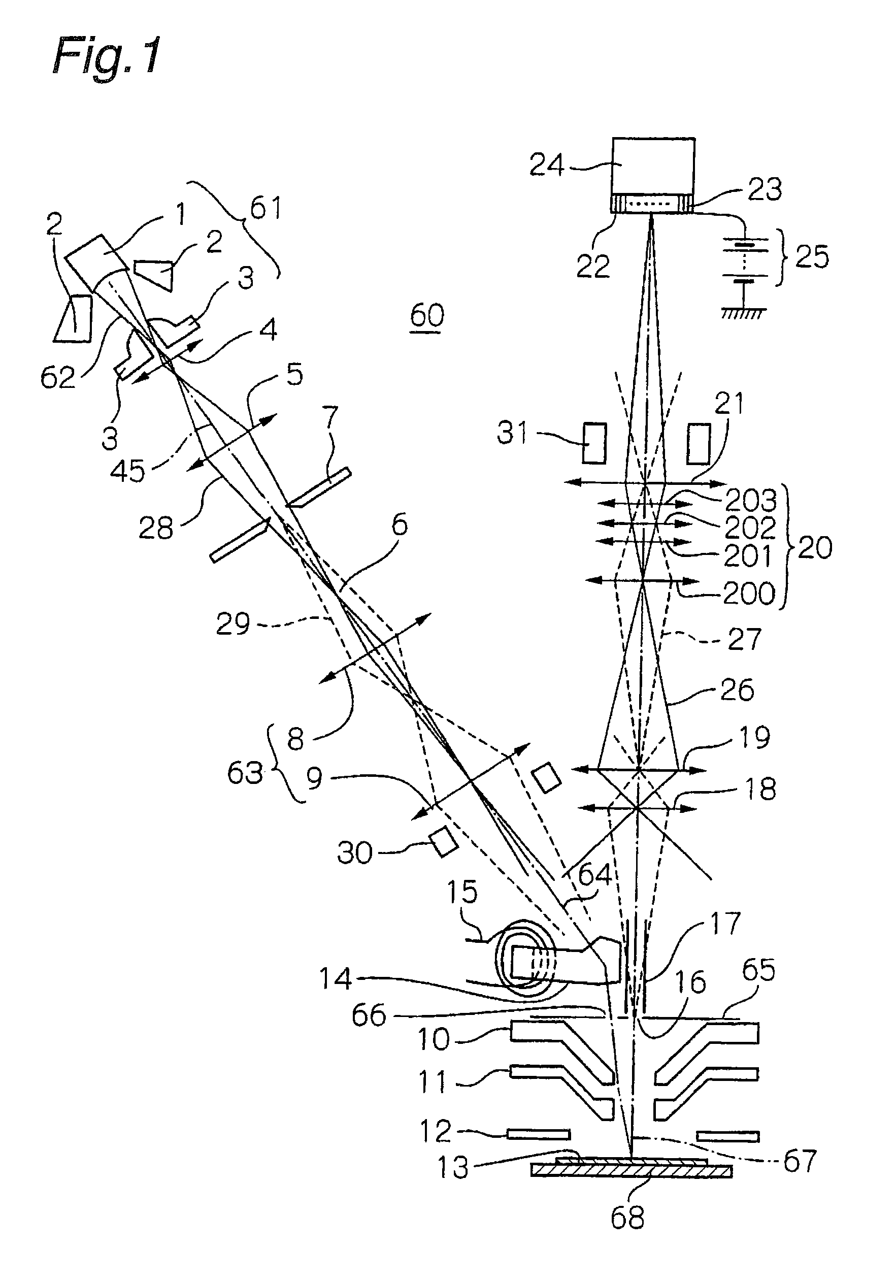
[0016]An electron beam apparatus using an image projection optical system requires a large flow of a primary electron beam. In this circumstance, the primary electron beam could result in a significantly blurred focus due to the space charge effect. To minimize the blurred focus of the primary beam caused by the space charge effect, an electron gun characterized by a lower brightness and a higher emittance, or (crossover diameter)×(beam emission angle) is required. In addition, it has been difficult with an electron gun constructed with a Pierce type electron gun for a purpose of generating an X-ray to converge the beams to achieve a current density of 500 A / cm2 or higher. The present invention has been made to solve the above-pointed problems and an object thereof is to provide an electron gun allowing for the low brightness and high emittance as well as an electron gun for producing a large-current narrowly converged primary electron beam.
[0039]According to the present invention, it becomes possible to improve a resolution by a charged particle beam optical system as a whole. In addition, since an aperture angle can be made larger, while maintaining a substantially same level of resolution as that achieved by the conventional technologies, therefore a beam transmission rate can be higher, which in turn contributes to the increased throughput by increasing a volume of signal without increasing an illumination current, over a defect inspection apparatus using an image projection optical system applied with the charged particle beam according to the conventional technologies.

Problems solved by technology

In this circumstance, the primary electron beam could result in a significantly blurred focus due to the space charge effect.
In addition, it has been difficult with an electron gun constructed with a Pierce type electron gun for a purpose of generating an X-ray to converge the beams to achieve a current density of 500 A / cm2 or higher.
To cope with this failure, such a problem may arise in that if simply the object plane position and the image plane position are established out of a filter, a double symmetry of the trajectory can not be ensured but a second-order geometric aberration would be newly introduced by the filter, resulting in an adversely increased off-axis aberration of the entire optical system including an aberration correction optical apparatus.
However, even with such an arrangement employed, the off-axis aberration could still be increased.

Method used


Image

  • Electron beam apparatus and an aberration correction optical apparatus
  • Electron beam apparatus and an aberration correction optical apparatus
  • Electron beam apparatus and an aberration correction optical apparatus

Examples


second embodiment

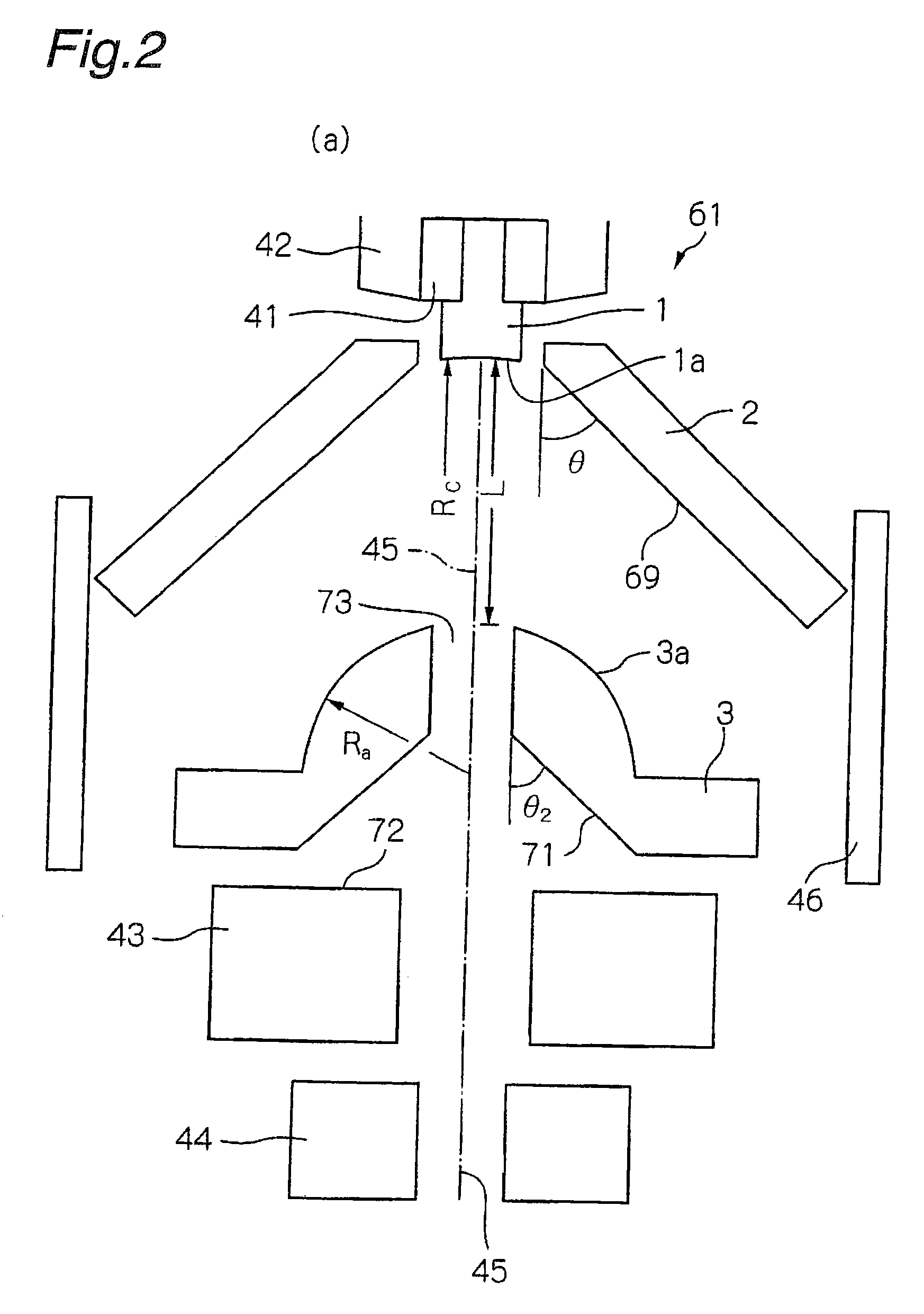
[0067]the present invention is configured such that the relationship among the distance L along the optical axis between the curved surface (the first sphere) 1a defining the electron emission surface of the cathode and the convex surface (the second sphere) 3a of the drawing electrode, the radius of curvature, Rc, of the curved surface (the first sphere) 1a and the radius of curvature, Ra, of the convex surface (the second sphere) 3a satisfies an inequity defined by:

2Rc<L+Ra  (2)

third embodiment

[0068]the present invention is configured such that the relationship among the distance L along the optical axis between the curved surface (the first sphere) 1a defining the electron emission surface of the cathode and the convex surface (the second sphere) 3a of the drawing electrode, the radius of curvature, Rc, of the curved surface (the first sphere) 1a and the radius of curvature, Ra, of the convex surface (the second sphere) 3a satisfies an inequity defined by:

2Ra<Rc−L  (3)

[0069]For the Pierce type electron gun, which satisfies an equation defined by L=Rc−Ra, the curvature surface (the first sphere) 1a and the curvature surface (the second sphere) 3a represent concentric spheres. As obviously seen from the comparison to that, the cathode-anode distance L defined by the above inequity (1) is longer than a difference between the radii of concentric spheres. FIG. 7 shows a graphical representation of a beam property from a simulation taking the Rc=5 mm, Ra=2 mm and L=4 mm in ...

first embodiment

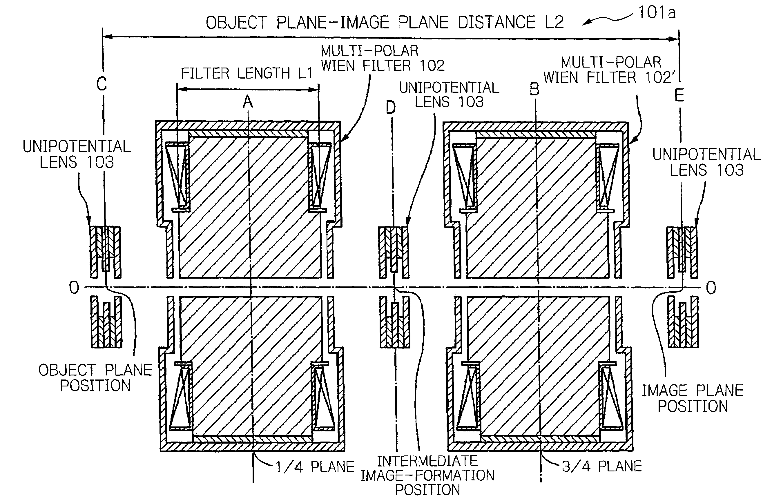
[0083]This allows the G trajectory to have a more ideal double symmetry over the present invention. Further in this configuration, since a deflector can be placed in the intermediate image-formation plane, the load to the power supply can be reduced preferably to the first example of the present invention.

[0084]It is to be noted also with this embodiment that each of the unipotential lenses 103a may be constructed in the multi-polar structure by overlapping dipolar or quadrupolar fields to serve for providing axial adjustment and for compensating for a gap resulting from a magnification scale. Although, instead of the unipotential lens 103a, a rotationally symmetric lens or an electromagnetic lens having the multi-polar structure may be employed, the electrostatic type may be more preferably employed from the consideration of the rotational effect on the image. As is the case with the previous embodiment, none of the unipotential lenses are necessarily rotationally symmetric lenses ...


PUM


Abstract

An electron beam apparatus for providing an evaluation of a sample, such as a semiconductor wafer, that includes a micro-pattern with a minimum line width not greater than 0.1 μm with high throughput. A primary electron beam generated by an electron gun is irradiated onto a sample and secondary electrons emanating from the sample are formed into an image on a detector by an image projection optical system. An electron gun 61 has a cathode 1 and a drawing electrode 3, and an electron emission surface 1a of the cathode defines a concave surface. The drawing electrode 3 has a convex surface 3a composed of a partial outer surface of a second sphere facing the electron emission surface 1a of the cathode and an aperture 73 formed through the convex surface for passage of the electrons. An aberration correction optical apparatus comprises two identically sized multi-polar Wien filters arranged such that their centers are in alignment with a ¼ plane position and a ¾ plane position, respectively, along an object plane-image plane segment in the aberration correction optical apparatus, and optical elements having bidirectional focus disposed in an object plane position, an intermediate image-formation plane position and an image plane position, respectively, in the aberration correction optical apparatus.

Description

BACKGROUND OF THE INVENTION[0001]1. Technical Field[0002]The present invention relates to an electron beam apparatus for providing an evaluation of a sample, such as a semiconductor wafer, that has a pattern with a minimum line width not greater than 0.1 μm with a high throughput, and further to an electron beam apparatus for irradiating a sample (i.e., a target), such as a part of a semiconductor wafer, with an electron beam having a large current density.[0003]The present invention also relates to an aberration correction optical apparatus for a charged particle beam optical system, and more specifically, to an aberration correction optical apparatus comprising a plurality of multi-polar Wien filters and operable to compensate for an aberration in an optical system using a charged particle beam, such as an electron beam, as well as to an image projection optical system and a scanning type optical system, both of which are incorporated with the same apparatus.[0004]2. Background Ar...

Claims


Application Information

Patent Timeline
Patent Type & Authority Patents(United States)
IPC IPC(8): G21K1/08H01J3/14H01J3/26
CPCH01J37/065H01J37/153H01J2237/061H01J2237/28H01J2237/083H01J2237/1534H01J2237/24592H01J2237/06375H01L21/00H01L21/02
Inventor HATAKEYAMA, MASAHIROMURAKAMI, TAKESHINOJI, NOBUHARUNAKASUJI, MAMORUSOBUKAWA, HIROSIMORI, SATOSHIKARIMATA, TSUTOMUYAMAZAKI, YUICHIRONAGAHAMA, ICHIROTA
Owner EBARA CORP
Learn More