

Wave absorber and manufacturing method of wave absorber
a manufacturing method and technology of absorber, applied in the direction of printed circuit manufacturing, printed circuit assembling, structural forms of radiation elements, etc., can solve the problems of increased weight, fluctuation of absorption properties, and increased thickness, and achieve effective absorption of em waves, high reflection attenuation properties, and sufficient reflection attenuation performance
- Summary
- Abstract
- Description
- Claims
- Application Information
AI Technical Summary
Benefits of technology
Problems solved by technology
Method used
Image

Examples
first embodiment
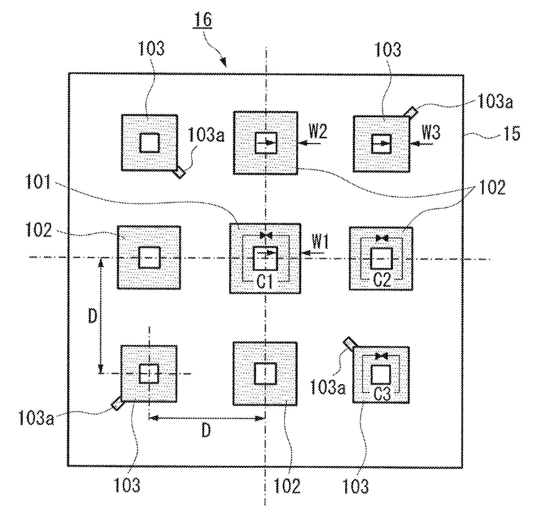
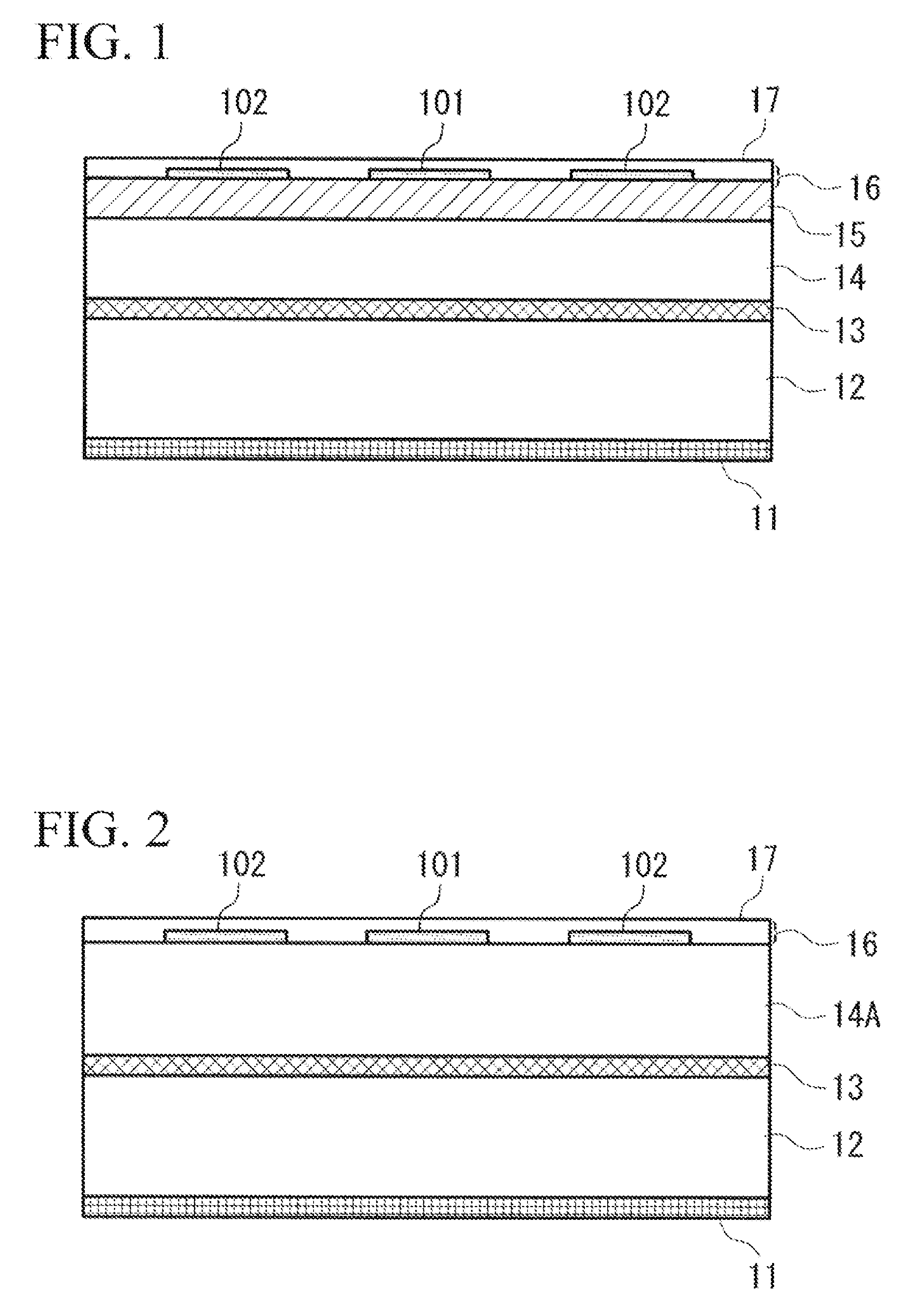
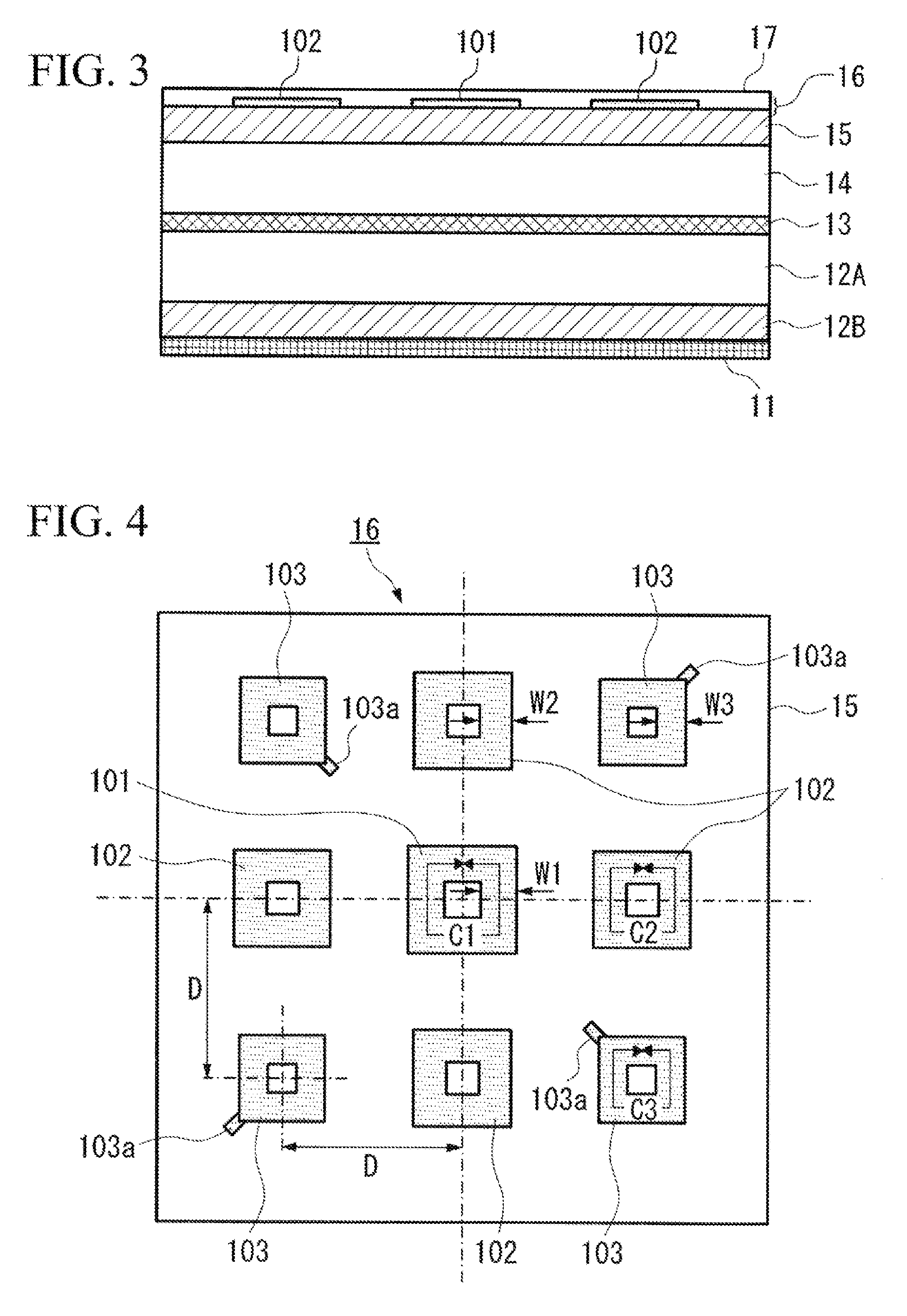
[0221]FIG. 1 is a sectional drawing showing the schematic configuration of a wave absorber which is a first embodiment of the present invention. The wave absorber of the present embodiment is configured by sequential lamination of a grid-like conductor layer 11 formed by copper foil (i.e. an electric conductor) of 12 μm thickness, a polycarbonate substrate 12 of 1.7 mm thickness constituting a first dielectric layer, a high-resistance conductor layer 13 having a surface resistance value (sheet resistance value) of 400 Ω / □, a laminate of a polycarbonate substrate 14 of 1.3 mm thickness constituting a second dielectric layer A and a BT (bismaleimide-triazine) substrate 15 of 0.3 mm thickness constituting a second dielectric layer B, a pattern layer 16 where multiple loop patterns of differing shape formed by copper foil of 12 μm thickness are cyclically disposed, and PET (polyethylene terephthalate) 17 with of 0.1 mm thickness that serves as a protective layer. Here, the grid-like con...
second embodiment
[0231]FIG. 6 is a sectional view showing the schematic configuration of a wave absorber, which is a second embodiment of the present invention. The wave absorber of the present embodiment is configured by sequential lamination of a grid-like conductor layer 21 formed by copper foil (i.e. an electric conductor) of 12 μm thickness, a polycarbonate substrate 22 of 1.5 mm thickness constituting a first dielectric layer, a high-resistance conductor layer 23 having a surface resistance value (sheet resistance value) of 400 Ω / □, a laminate of a polycarbonate substrate 24 of 1.1 mm thickness constituting a second dielectric layer A and a BT (bismaleimide-triazine) substrate 25 of 0.3 mm thickness constituting a second dielectric layer B, and a pattern layer 26 where multiple loop patterns of differing shape formed by copper foil of 12 μm thickness are cyclically disposed. Here, the grid-like conductor layer 21 and the high-resistance conductor layer 23 are identical to the grid-like conduct...
third embodiment
[0235]FIG. 9 is a sectional view showing the schematic configuration of a wave absorber, which is a third embodiment of the present invention. The wave absorber of the present embodiment is configured by sequential lamination of a conduct layer 31 formed by copper foil (i.e. an electric conductor) of 12 μm thickness, a polycarbonate substrate 32 of 0.7 mm thickness constituting a first dielectric layer, a polypropylene substrate 33 of 1.3 mm thickness where 20 weight parts of carbon powder constituting a dielectric loss layer are dispersed, and made to foam 3.8-fold, a laminate of a polycarbonate substrate 34 of 0.4 mm thickness constituting a second dielectric layer A and a BT (bismaleimide-triazine) substrate 35 of 0.3 mm thickness constituting a second dielectric layer B, and a pattern layer 36 where multiple loop patterns of differing shape formed by copper foil of 12 μm thickness are cyclically disposed. Here, as a carbon-dispersed foam substrate is used as the dielectric loss ...
PUM
| Property | Measurement | Unit |
|---|---|---|
| resistance | aaaaa | aaaaa |
| resistance | aaaaa | aaaaa |
| wavelength | aaaaa | aaaaa |
Abstract
Description
Claims
Application Information