
Method of fabricating power semiconductor device

a technology of power semiconductor and manufacturing method, which is applied in the direction of semiconductor devices, basic electric elements, electrical equipment, etc., can solve the problems of increased manufacturing cost, reduced production efficiency, and already reached process limitations in the layout design, so as to achieve economic and convenient formation, the effect of increasing the breakdown voltag

Inactive Publication Date: 2011-01-11
ANPEC ELECTRONICS CORPORATION
View PDF10 Cites 4 Cited by
  • Summary
  • Abstract
  • Description
  • Claims
  • Application Information

AI Technical Summary

Benefits of technology

The present invention provides a method of fabricating power semiconductor devices that improves uniformity of electric field and increases breakdown voltage. The method involves etching a substrate to form trenches, depositing a gate insulating layer to cover the substrate and the trenches, and performing an ion implantation process to form a base in the substrate. A second deposition process is performed to form a second gate material layer that fills the trenches and covers the gate insulating layer. An anisotropic etching back process is performed to partially remove the gate material layer and expose the gate insulating layer. A second ion implantation process is performed to form a second dopant layer in the substrate. A drive-in process is performed to extend the distribution of the dopants in the substrate to form a bottom-lightly-doped layer surrounding the bottom of the trench. The bottom-lightly-doped layer solves the problem of non-uniform electric field and protects the bottom of the gate trench from damage, increasing the breakdown voltage. The method is economical and convenient to implement without additional masks.

Problems solved by technology

However, the layout design already reaches the process limitation.
For example, there is a process limitation for the contact plug electrically connecting the gate, such that the opening for forming the contact plug must have a certain width for filling with material such as tungsten to form the contact plug.
However, the reliability is affected.
However, in the conventional process for forming such guard ring doped region, a mask is required to cover the region other than the guard ring doped region, resulting in an increased manufacturing cost, which is described in detail as follows.
Especially, in step 2, a mask is required for forming a guard ring doped region, and it is costly.

Method used


Image

  • Method of fabricating power semiconductor device
  • Method of fabricating power semiconductor device
  • Method of fabricating power semiconductor device

Examples


Embodiment Construction

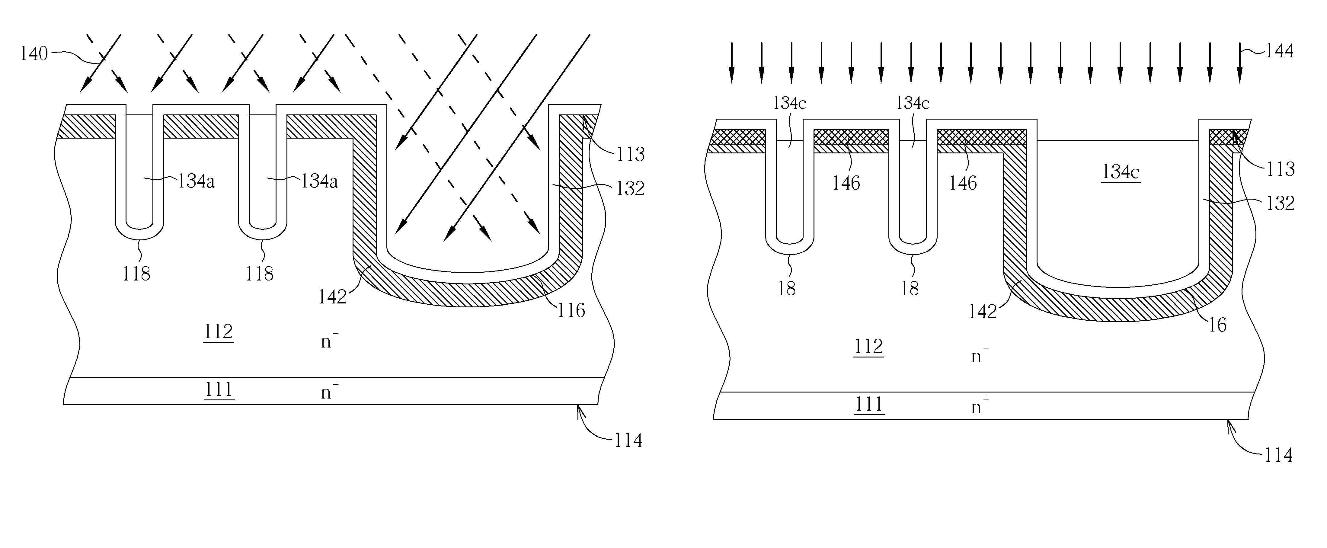
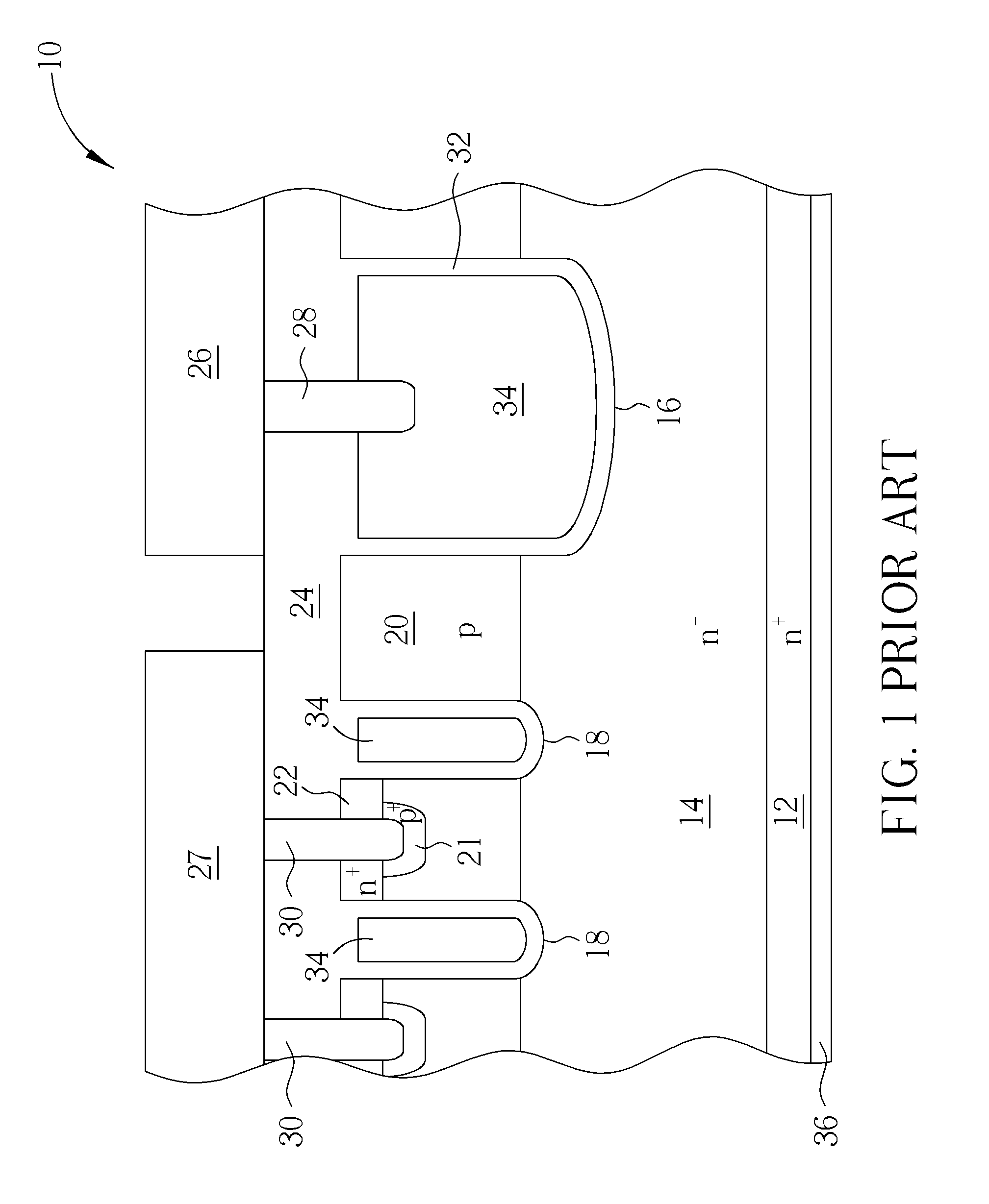
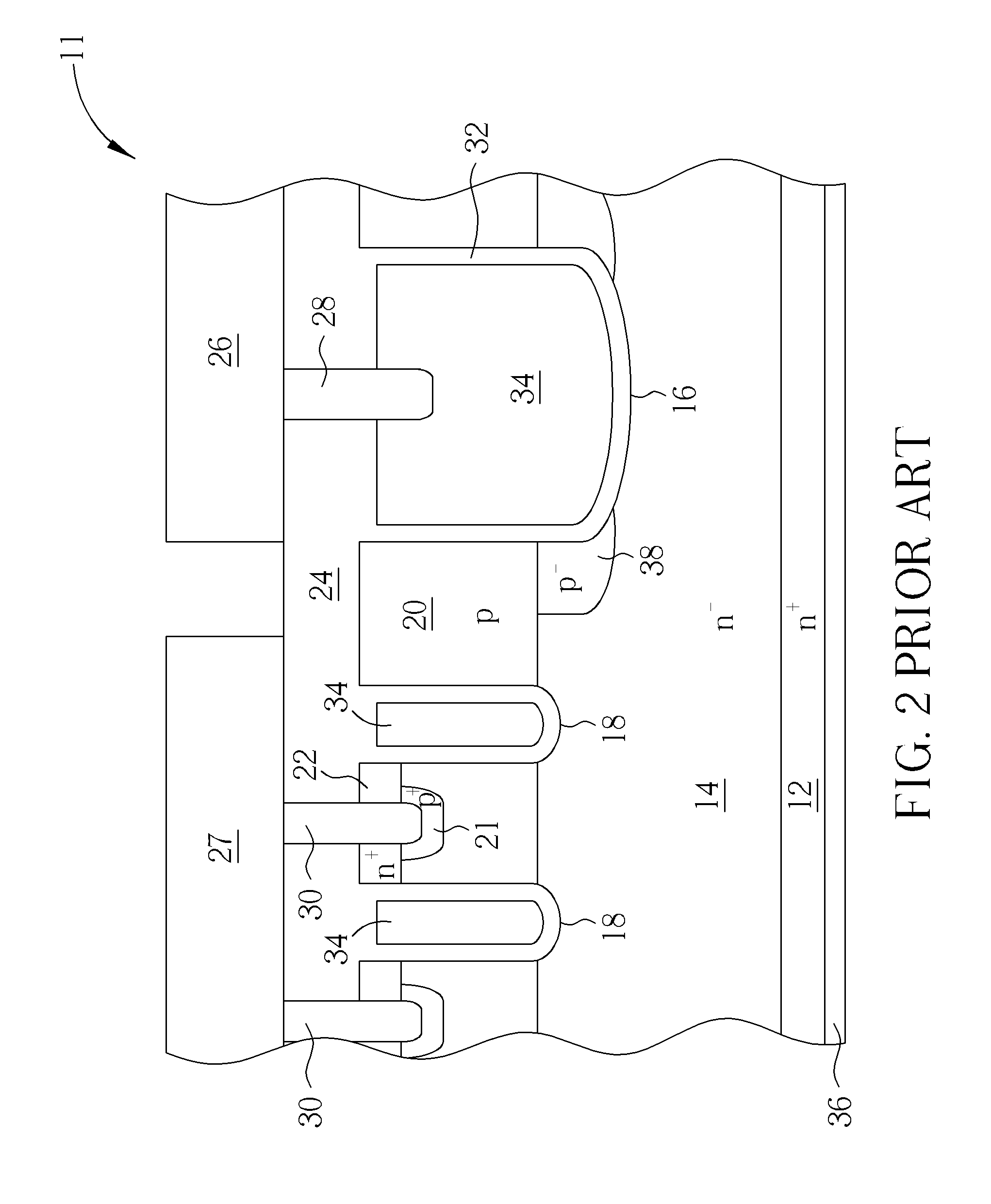
[0018]FIG. 4 is a flow chart of main steps utilizing masks in a method of fabricating a power device according to the present invention, which may be compared with the conventional flow chart of main steps as shown in FIG. 3. After the active area is defined, the conventional step 2 for forming the guard ring using a mask is not performed but the step 3 is performed instead to form gate trenches and then to fill the gate trench with the gate material. The filling of the gate material is accomplished by steps 101, 102, and 103. That is, in step 101, the first deposition of gate material and etching back are performed; in step 102, a tilt ion implantation for subsequently forming a bottom-lightly-doped layer is performed; and, in step 103, the second deposition of gate material and etching back are performed. After the filling of the gate trenches, a formation of a base (for example the formation of a p base) may be further performed, in which the dopant of step 102 and the dopant of ...


PUM


Abstract

Wider and narrower trenches are formed in a substrate. A first gate material layer is deposited but not fully fills the wider trench. The first gate material layer in the wider trench and above the substrate original surface is removed by isotropic or anisotropic etching back. A first dopant layer is formed in the surface layer of the substrate at the original surface and the sidewall and bottom of the wider trench by tilt ion implantation. A second gate material layer is deposited to fully fill the trenches. The gate material layer above the original surface is removed by anisotropic etching back. A second dopant layer is formed in the surface layer of the substrate at the original surface by ion implantation. The dopants are driven-in to form a base in the substrate and a bottom-lightly-doped layer surrounding the bottom of the wider trench and adjacent to the base.

Description

BACKGROUND OF THE INVENTION[0001]1. Field of the Invention[0002]The present invention relates to a method of manufacturing a power device, and more particularly, to a method for manufacturing a power semiconductor device capable of improving uniform distribution of electric field.[0003]2. Description of the Prior Art[0004]Power devices are typical semiconductor devices in power management applications, such as a switching power supply, a power control IC of a computer system or peripherals, a power supply of a backlight, motor controller, etc. Power devices can include various kinds of transistors, such as an insulated gate bipolar transistor (IGBT), a metal-oxide-semiconductor field effect transistor (MOSFET) and a bipolar junction transistor (BJT).[0005]Furthermore, developments of trench power MOSFETs become an important tendency, because trench power MOSFETs can provide a lower electric resistance in conduction and a smaller device dimension, and can effectively control voltages...

Claims


Application Information

Patent Timeline
Patent Type & Authority Patents(United States)
IPC IPC(8): H01L21/336
CPCH01L21/26586H01L29/1095H01L29/4236H01L29/66727H01L29/66734H01L29/7811H01L29/7813H01L21/26513
Inventor LIN, WEI-CHIEHHSU, HSIN-YUYANG, GUO-LIANGYEH, JEN-HAO
Owner ANPEC ELECTRONICS CORPORATION
Features
  • Generate Ideas
  • Intellectual Property
  • Life Sciences
  • Materials
  • Tech Scout
  • Unparalleled Data Quality
  • Higher Quality Content
  • 60% Fewer Hallucinations
Learn More