

Enhancement-mode field effect transistor based electrostatic discharge protection circuit
a protection circuit and enhancement-mode technology, applied in the direction of amplifier protection circuit arrangements, circuit arrangements, amplifiers, etc., can solve the problems of adversely affecting the performance of rf circuits, circuitry for gallium arsenide phemt technology that is currently in use, and undesirable characteristics of circuitry, so as to maximize the linearity of the esd clamp circuit and minimize parasitic capacitance.
Active Publication Date: 2011-02-01
QORVO US INC
View PDF10 Cites 24 Cited by
- Summary
- Abstract
- Description
- Claims
- Application Information
AI Technical Summary
Benefits of technology
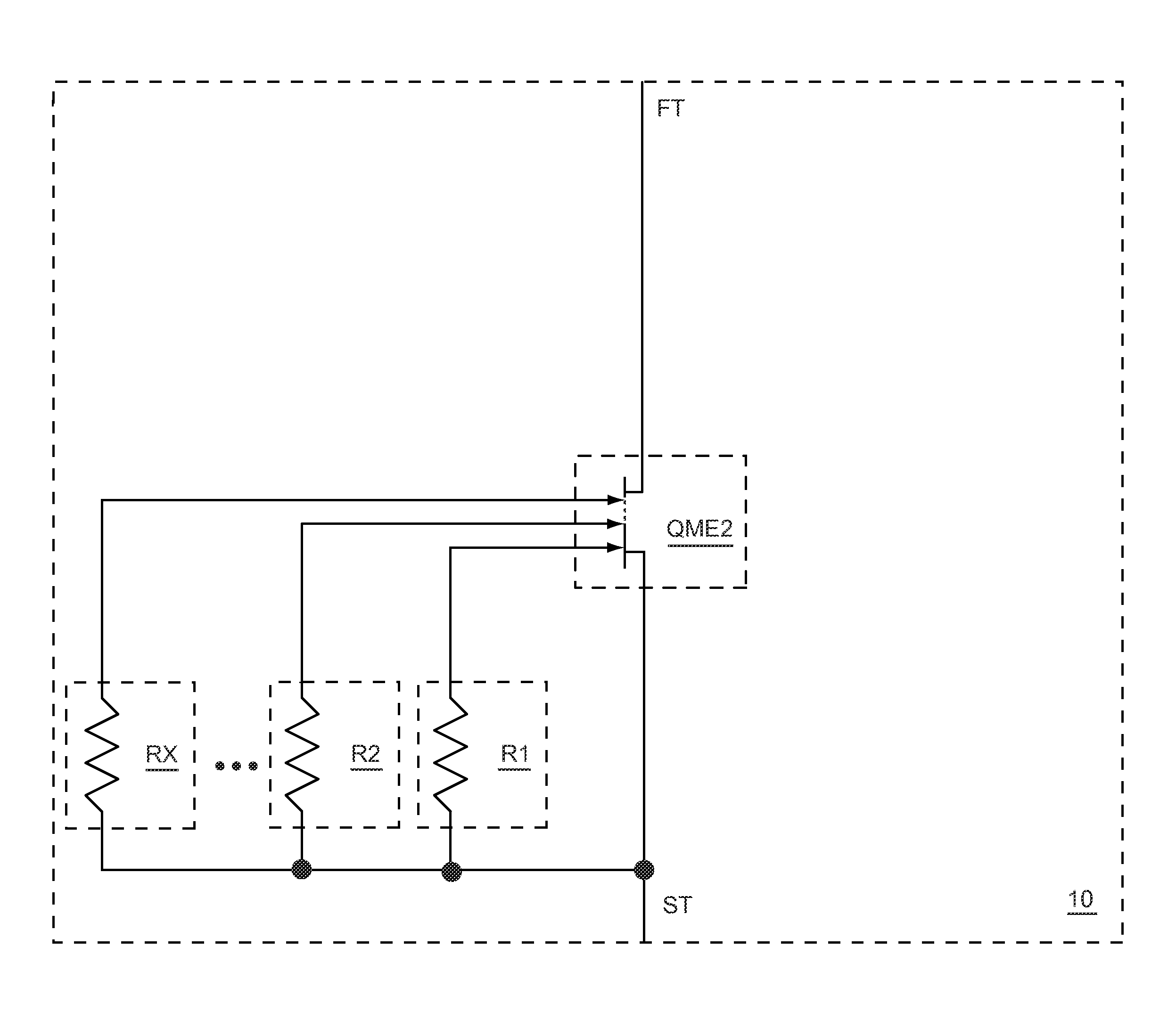
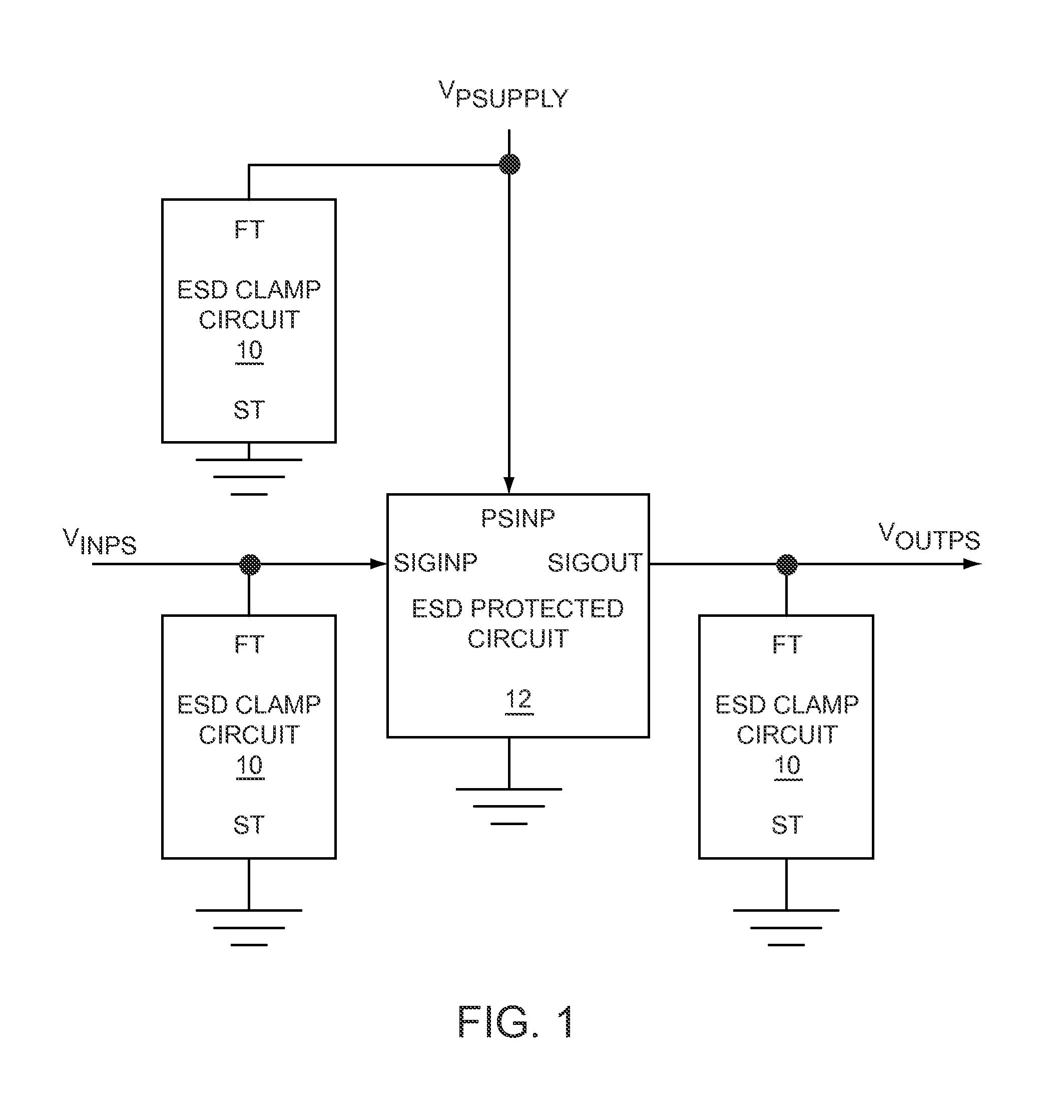
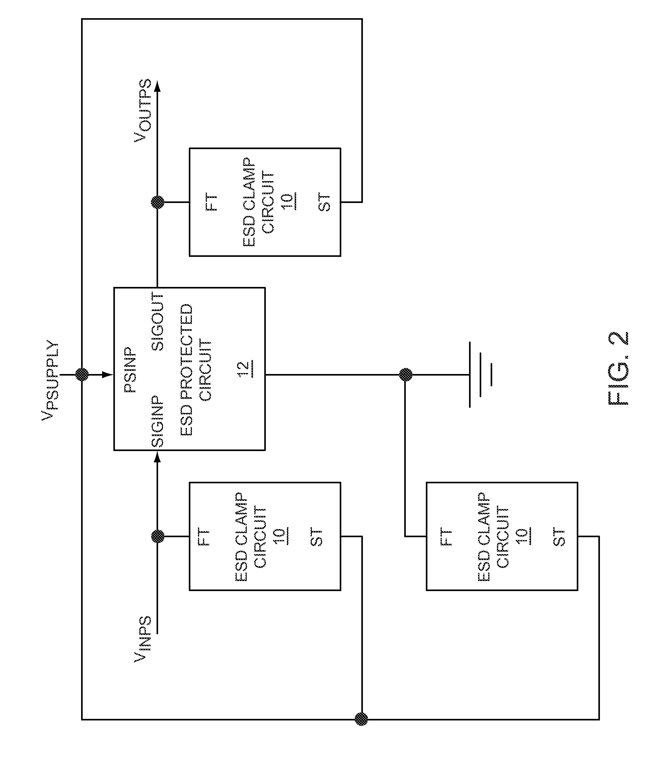
The present invention is about an electrostatic discharge (ESD) clamp circuit that protects other circuitry from high voltage ESD events. The circuit uses a field effect transistor (FET) element as a clamping element, which is triggered by a drain-to-gate capacitance or a drain-to-gate resistance. The FET element may be a small and simple circuit, which minimizes parasitic capacitances and maximizes linearity over a wide frequency range. The FET element may be made of compound semiconductor materials like Gallium Arsenide, Indium Phosphide, Gallium Nitride, or any combination thereof. The invention also includes enhancement-mode devices that require a positive gate bias to turn on. The invention has various aspects and can be used in various electronic devices.
Problems solved by technology
Electrostatic discharge (ESD), which is a large subset of electrical overstress (EOS), is a major reliability issue in integrated circuits (ICs).
As semiconductor devices have scaled to smaller dimensions and ICs have become more complex, the potential for destructive ESD events has become more serious.
However, ESD protection circuitry for Gallium Arsenide pHEMT technology that is currently in use provides undesirable characteristics.
Gallium Arsenide pHEMT ESD protection structures may have unwanted parasitic capacitances and resistances which may adversely affect performance of RF circuits.
At RF frequencies, the parasitics associated with the ESD protection structures can lead to impedance mismatches, which may cause signal reflection that degrades the performance of the circuit that it is protecting.
Method used
View moreImage
Smart ImageViewing Examples

Examples
first embodiment
[0014]FIG. 5 shows details of the ESD clamp circuit, which includes an enhancement-mode field effect transistor (FET) element and a first resistive element coupled between a gate and a source of the enhancement-mode FET element, according to the ESD clamp circuit.
second embodiment
[0015]FIG. 6 shows a series resistive element coupled in series with the enhancement-mode FET element illustrated in FIG. 5, according to the ESD clamp circuit.
third embodiment
[0016]FIG. 7 shows multiple enhancement-mode FET elements coupled in series, of the ESD clamp circuit.
Login to View More PUM
 Abstract
The present invention relates to an electrostatic discharge (ESD) clamp circuit that is used to protect other circuitry from high voltage ESD events. The ESD clamp circuit may include a field effect transistor (FET) element as a clamping element, which is triggered by using a drain-to-gate capacitance, a drain-to-gate resistance, or both of the FET element, and a resistive element as a voltage divider to divide down an ESD voltage to provide a triggering gate voltage of the FET element. In its simplest embodiment, the ESD clamp circuit includes only an FET element and a resistive element. Therefore, the single FET element ESD clamp circuit may be small compared to other ESD protection circuits. The simplicity of the ESD clamp circuit may minimize parasitic capacitances, thereby maximizing linearity of the ESD clamp circuit over a wide frequency range.
Description
CROSS-REFERENCE TO RELATED APPLICATIONS[0001]This application is related to U.S. patent application Ser. No. 11 / 609,497 entitled ON-CHIP ESD PROTECTION CIRCUIT FOR RADIO FREQUENCY (RF) INTEGRATED CIRCUITS filed Dec. 12, 2006, the disclosure of which is hereby incorporated herein by reference in its entirety.FIELD OF THE INVENTION[0002]The present invention relates to electrostatic discharge (ESD) protection circuits, which may be used to protect other circuits from the high voltages associated with ESD events.BACKGROUND OF THE INVENTION[0003]Electrostatic discharge (ESD), which is a large subset of electrical overstress (EOS), is a major reliability issue in integrated circuits (ICs). As semiconductor devices have scaled to smaller dimensions and ICs have become more complex, the potential for destructive ESD events has become more serious. More recently, there has been a tremendous demand for increasing the ESD robustness of Radio Frequency (RF) ICs, especially for wireless applica...
Claims
Login to View More Application Information
Patent Timeline
 Patent Type & AuthorityPatents(United States)
IPC IPC(8): H02H3/22
CPCH01Q1/50H03F1/52H03F2200/441
InventorLI, JASON YUXINWOHLMUTH, WALTER A.MUTHUKRISHNAN, SWAMINATHANIVERSEN, CHRISTIAN RYEPEACHEY, NATHANIEL
OwnerQORVO US INC