Nanolithography methods and products therefor and produced thereby
- Summary
- Abstract
- Description
- Claims
- Application Information
AI Technical Summary
Benefits of technology
Problems solved by technology
Method used
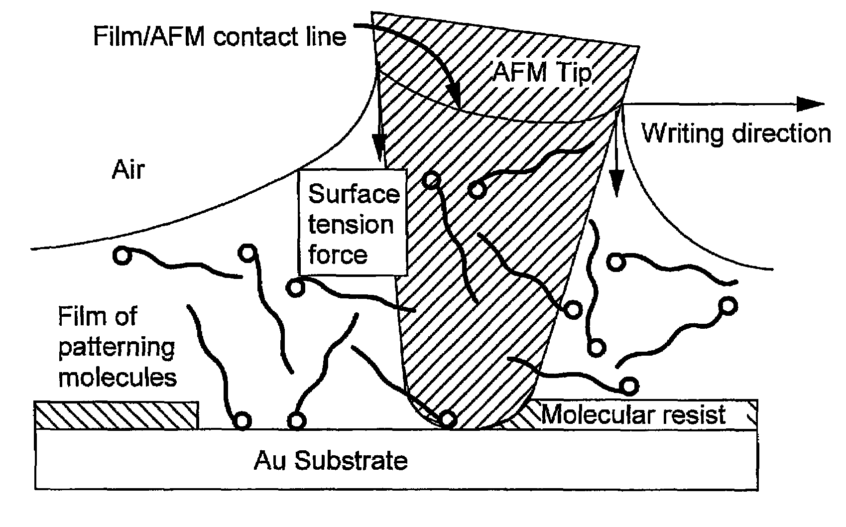
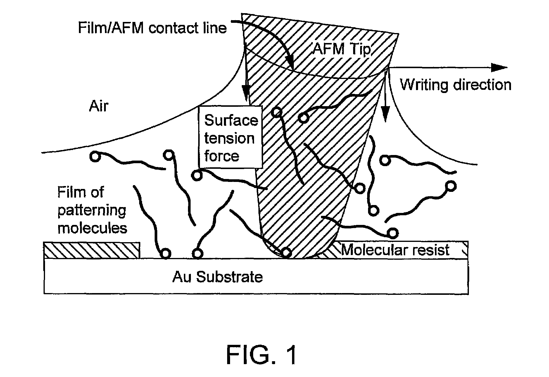
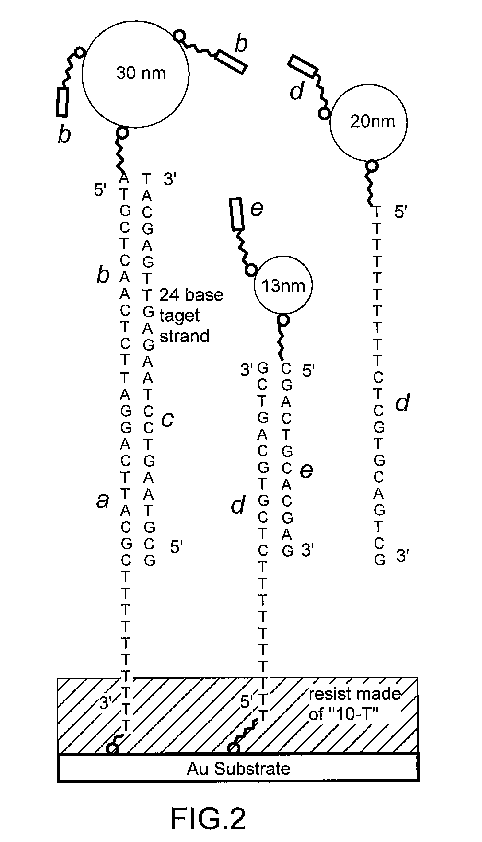
Image

Examples
example 1
Preparation of a Three-Dimensional Structure on a Gold Substrate Using Meniscus Force Nanografting
Gold substrates were prepared as follows. Polished single-crystalline Si(100) wafers were coated with 5 nm of Ti, followed by at least 10 nm of Au by thermal evaporation. The Si(100) wafers (4″ diameter (1-0-0) wafers; 3-4.9 ohm / cm resistivity; 500-550 μm thickness) were purchased from Silicon Quest International, Inc. (Santa Clara, Calif.). Thermal evaporation of 5 nm of Ti (99.99%; Alfa Aesar; Ward Hill, Mass.) followed by 10 nm of Au (99.99%; D. F. Goldsmith; Evanston, Ill.) was accomplished using an Edwards Auto306 Turbo Evaporator equipped with a turbopump (Model EXT510) and an Edwards FTM6 quartz crystal microbalance to determine film thickness. Au and Ti depositions were conducted at room temperature at a rate of 3 angstroms / second and a pressure of 10−7 torr.
The resist was composed of alkanethiol-oligonucleotides of the composition 5′-SH—(CH2)6-(T)10 (hereinafter “10-T”). 10-T w...
example 2
Preparation of a Three-Dimensional Structure on a Gold Substrate Using Nanograffing
Gold substrates were prepared as described in Example 1. The substrates were coated with a resist composed of a combination of 10-T and mercaptohexanol (MCH) (hereinafter the “10-T / MCH” resist). The 10-T / MCH resist was applied to the substrate as follows. First, 10-T was prepared, purified and applied to the substrate, all as described in Example 1. After washing the substrate with nanopure water and drying it with difluoroethane, it was placed in a closed container with a few drops of MCH (Aldrich) and left in the closed container for 3 hours at room temperature to apply the MCH by vapor deposition. After the three-hour incubation, the substrate was washed in ethanol and dried with difluoroethane.
Patterning compound A (preparation described in Example 1) was applied to the substrate by standard nanografting as described in Xu and Liu, Langmuir, 13, 127 (1997) with some modifications. In particular, t...
example 3
Preparation of a Three-Dimensional Structure on a Gold Substrate Using Meniscus Force Nanografting
Gold substrates were prepared and coated with 10-T resist as described in Example 1. Patterning compound A was prepared and applied to the substrate as described in Example 1. After application of patterning compound A, any bare substrate was coated with 10-T as described in Example 1, and the tip was rinsed with nanopure water and dried with difluoroethane.
Then, patterning compound D was prepared and applied to the substrate with the rinsed tip as described in Example 1, after which the substrate was again coated with 10-T resist as described in Example 1. Patterning compound D was identical to patterning compound A, except that the (N)12 sequence of oligonucleotide strand D was different than the (N)12 sequence of oligonucleotide strand A (see FIG. 2). Patterning compounds A and D were patterned in parallel lines less than 500 nm apart.
Structure-forming compounds B, C and E (see FIG. ...
PUM
 Abstract
Description
Claims
Application Information
 - R&D Engineer
- R&D Manager
- IP Professional
- Industry Leading Data Capabilities
- Powerful AI technology
- Patent DNA Extraction
Browse by: Latest US Patents, China's latest patents, Technical Efficacy Thesaurus, Application Domain, Technology Topic.
© 2024 PatSnap. All rights reserved.Legal|Privacy policy|Modern Slavery Act Transparency Statement|Sitemap