Method and system for verifying the equivalence of digital circuits

a digital circuit and equivalence technology, applied in the field of methods and systems for verifying the equivalence of digital circuit designs, can solve the problems that the enormous space of input signal values and internal states cannot be totally verified by logic simulation, and the ffv of the dut at the register-transfer level is inherently difficult to achieve when using automated methods

Inactive Publication Date: 2011-02-15
GLOBALFOUNDRIES INC
View PDF4 Cites 12 Cited by
  • Summary
  • Abstract
  • Description
  • Claims
  • Application Information

AI Technical Summary

Problems solved by technology

However, today's hardware designs are much more complex.
This enormous space of input signal values and internal states cannot be totally verified by logic simulation.
However, the FFV of the DUT at the register-transfer level is inherently difficult to achieve when using automated methods.
It is well-known that the time needed to design digital circuits is a critical issue in a modern chip design.
In such an instance, a problem often occurs when an existing and new design assume different design methodologies and a different tool set for creating the hardware.
For example, a problematic case may include the use of different HDLs, such as VHDL and Verilog.
Among other potential adaptations required when porting existing logic designs, the following typical problems can occur:a logic function needs to be moved from one pipeline stage to the next;the timing behaviour needs to be changed;asynchronous resets are not allowed in the new logic design but are used in the existing logic design;clock control signals need to be changed; andscan path chains and associated control signals require altering.
Available tools which can perform the equivalence checking of two logic designs at the RTL that includes sequential logic circuits face the problem of a potentially huge state space of a finite state machine represented by the logic designs.
This problem either restricts the verification coverage that can be achieved or it prevents the use of the so-called sequential equivalence checker tools in many real-world porting scenarios.
However, as described above, this is often not the case for logic designs ported from one semiconductor node to another and for reusing logic design components.

Method used


Image

  • Method and system for verifying the equivalence of digital circuits
  • Method and system for verifying the equivalence of digital circuits
  • Method and system for verifying the equivalence of digital circuits

Examples


Embodiment Construction

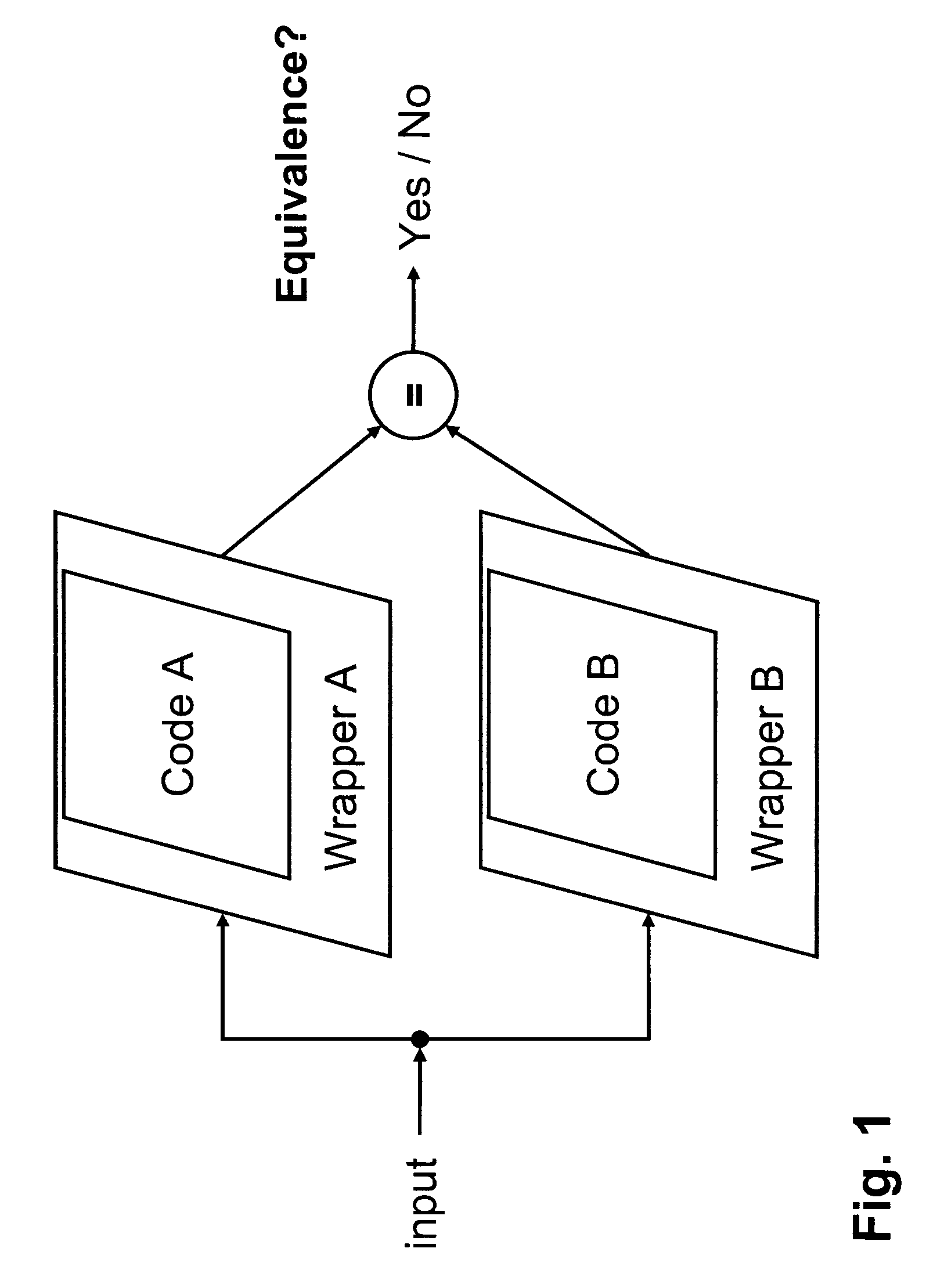
[0041]Referring to FIG. 1, there is shown is a block diagram of two designs represented by two HDL logic implementations (Code A and Code B) that serve as inputs to the system of the present invention, and which are to be compared for equivalence for a given input set.

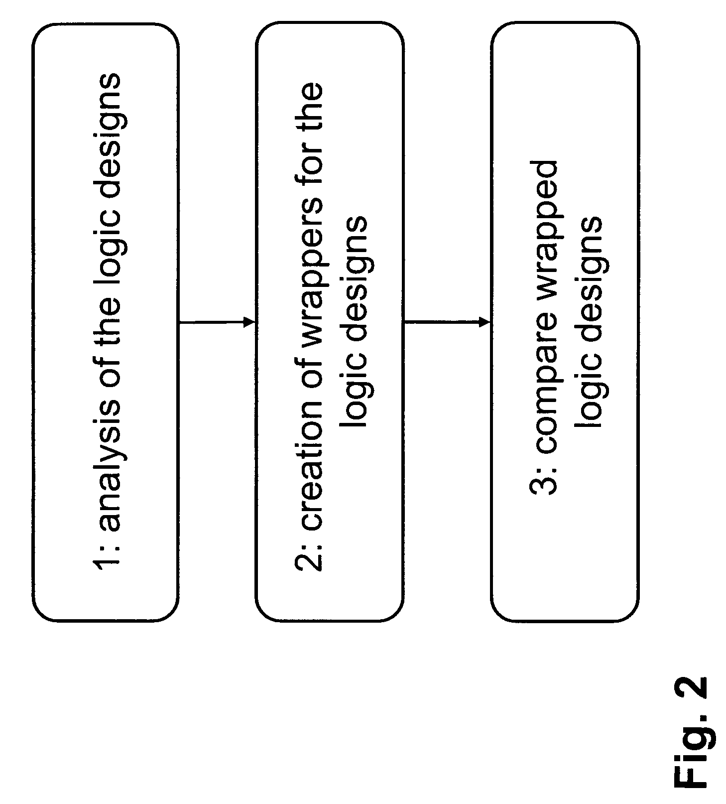
[0042]Referring to FIG. 2, there is shown a flow chart describing a preferred embodiment of the present invention. In step 1, two designs in need to be compared are analysed. This step is referred to as the analysis step. In step 2, a wrapper is constructed for each design based on the analysis results encapsulating the design. This step is referred to as the wrapper creation step. In step 3, the resulting two modified designs are compared for sequential equivalence. This step is referred to as the verification step. The verification step uses existing verification methods and tools known in the art. Their use is enabled by special wrappers created during the wrapper creation step.

[0043]The analysis and wrapper creatio...


PUM


Abstract

The automatic verification of designs of digital circuits for their equivalence, wherein logic designs implemented in different hardware description languages (HDLs) and different design methodologies are compared. The designs (Code A, Code B) are modified by adding special wrappers (Wrapper A, Wrapper B), and used to equalize the timing of pairs of selected input signals and selected output signals of the logic designs. The wrappers drive certain signals of the designs that are not relevant for actual comparison, such signals including clock signals, clock control signals, scan-path signals, scan-path control signals, and reset signals. In a preferred embodiment, HDL descriptions of logic designs are analyzed. Based on this analysis, the wrappers are implemented as changes to the HDL descriptions. In another embodiment, RTL and / or gate-level netlists are analyzed and modified.

Description

BACKGROUND OF THE INVENTION[0001]The present invention relates to a method and a system for verifying the equivalence of digital circuit designs.Logic Design Verification[0002]Digital logic circuits typically implement a logic function that represents the core of any computer or processing unit. Thus, before a logic design is constructed in real hardware, it must be tested, and the proper operation thereof has to be verified against the design specification. This task is called functional verification of a design under test (DUT) and is described in a paper by J. M. Ludden et al., entitled “Functional verification of the POWER4 microprocessor and POWER4 multiprocessor systems”, IBM Journal of Research and Development, Vol. 46, No. 1, January 2002.[0003]Functional verification is commonly performed at various levels of abstraction of the hardware design, e.g., a switch level and a transistor level. The switch level typically includes active circuit elements (e.g., transistors) and pa...

Claims


Application Information

Patent Timeline
Patent Type & Authority Patents(United States)
IPC IPC(8): G06F17/50G06F9/45
CPCG06F17/504G06F30/3323
Inventor GEMMEKE, TOBIASLEENSTRA, JENSMAEDING, NICOLASMONY, HARI
Owner GLOBALFOUNDRIES INC
Why Eureka
Try Eureka