Semiconductor contact barrier

a technology of contact barrier and semiconductor, applied in the direction of semiconductor devices, semiconductor/solid-state device details, electrical apparatus, etc., can solve the problems of unresolved problems of using copper as a contact, unwanted reaction with other materials, and contact resistance between the contact and the region to be contacted, so as to reduce the resistance of the device, improve the device performance, and reduce the contact resistance

Active Publication Date: 2011-03-01
TAIWAN SEMICON MFG CO LTD
View PDF23 Cites 6 Cited by
  • Summary
  • Abstract
  • Description
  • Claims
  • Application Information

AI Technical Summary

Benefits of technology

[0010]By using these methods to form the contacts described, the contact resistance between the contact and the region to be contacted can be reduced. This will result in an overall reduction in the resistance of the device, and, accordingly, better performance of the device.

Problems solved by technology

However, the use of copper has some inherent problems that must be overcome, such as copper's propensity to migrate and cause unwanted reactions with other materials.
However, this solution, while an improvement over previous methods, does not by itself solve the problems with using copper as a contact.
These unfilled grain boundaries increase the potential contact resistance, making this solution less desirable.

Method used


Image

  • Semiconductor contact barrier
  • Semiconductor contact barrier
  • Semiconductor contact barrier

Examples


Embodiment Construction

[0017]The making and using of the presently preferred embodiments are discussed in detail below. It should be appreciated, however, that the present invention provides many applicable inventive concepts that can be embodied in a wide variety of specific contexts. The specific embodiments discussed are merely illustrative of specific ways to make and use the invention, and do not limit the scope of the invention.

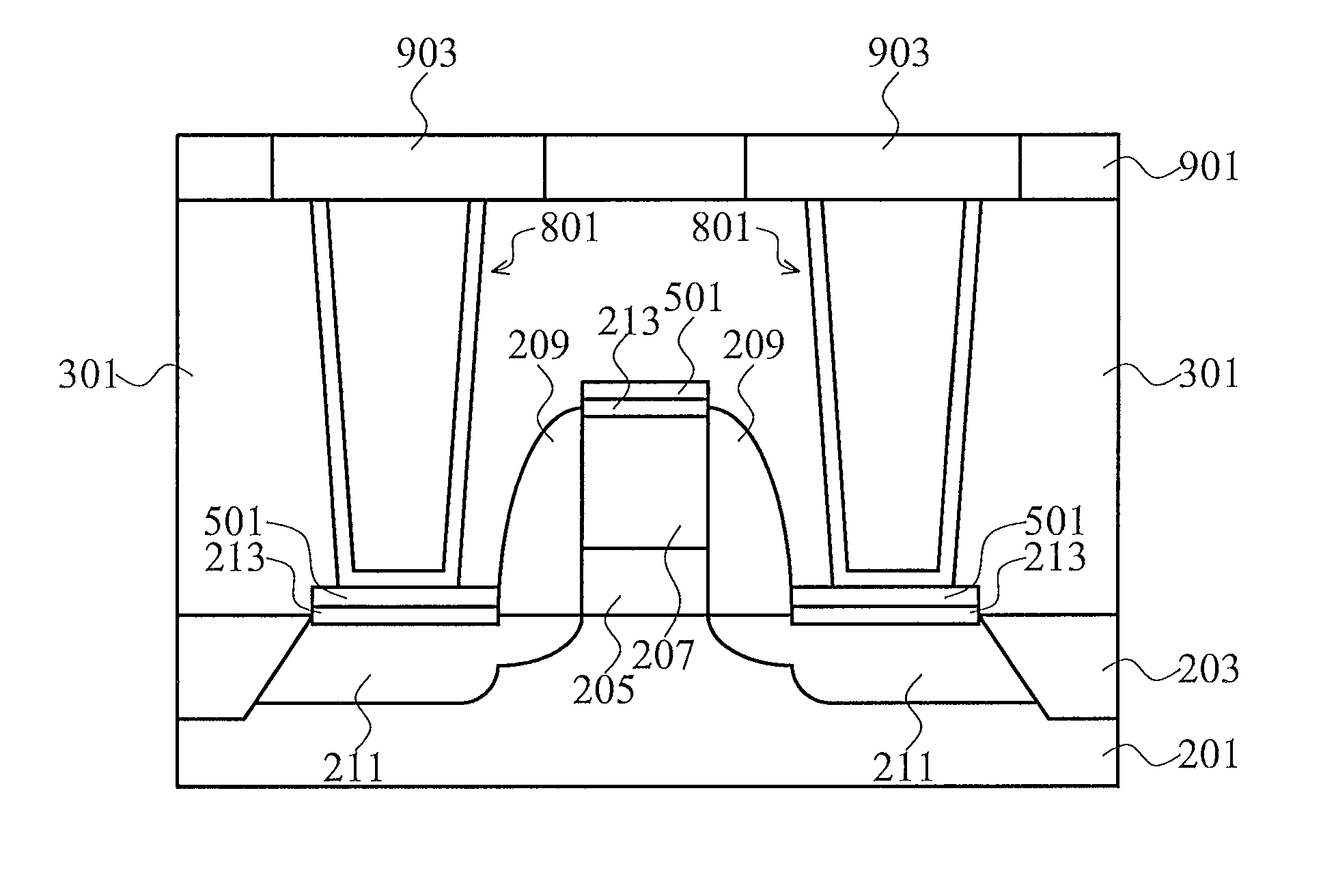
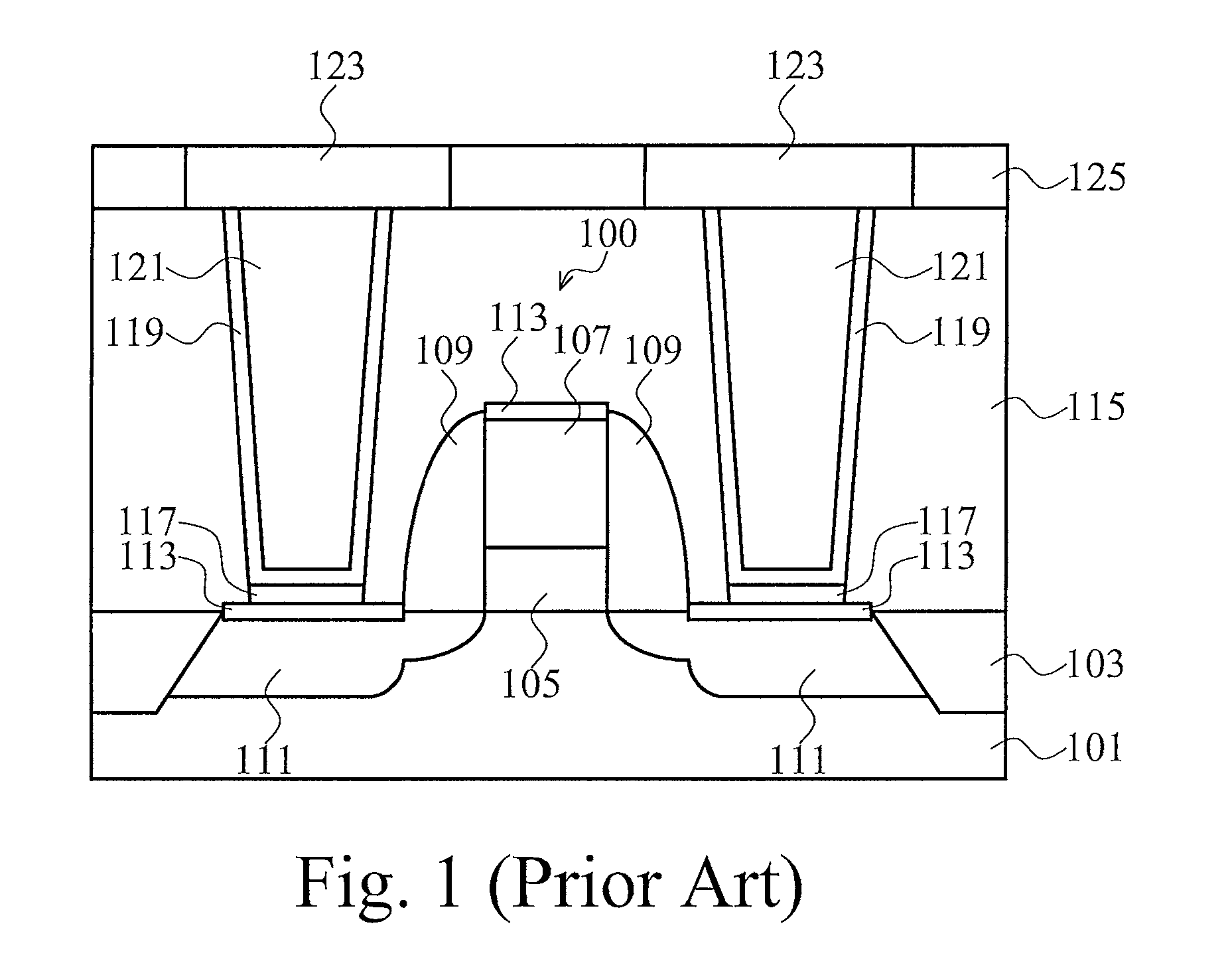
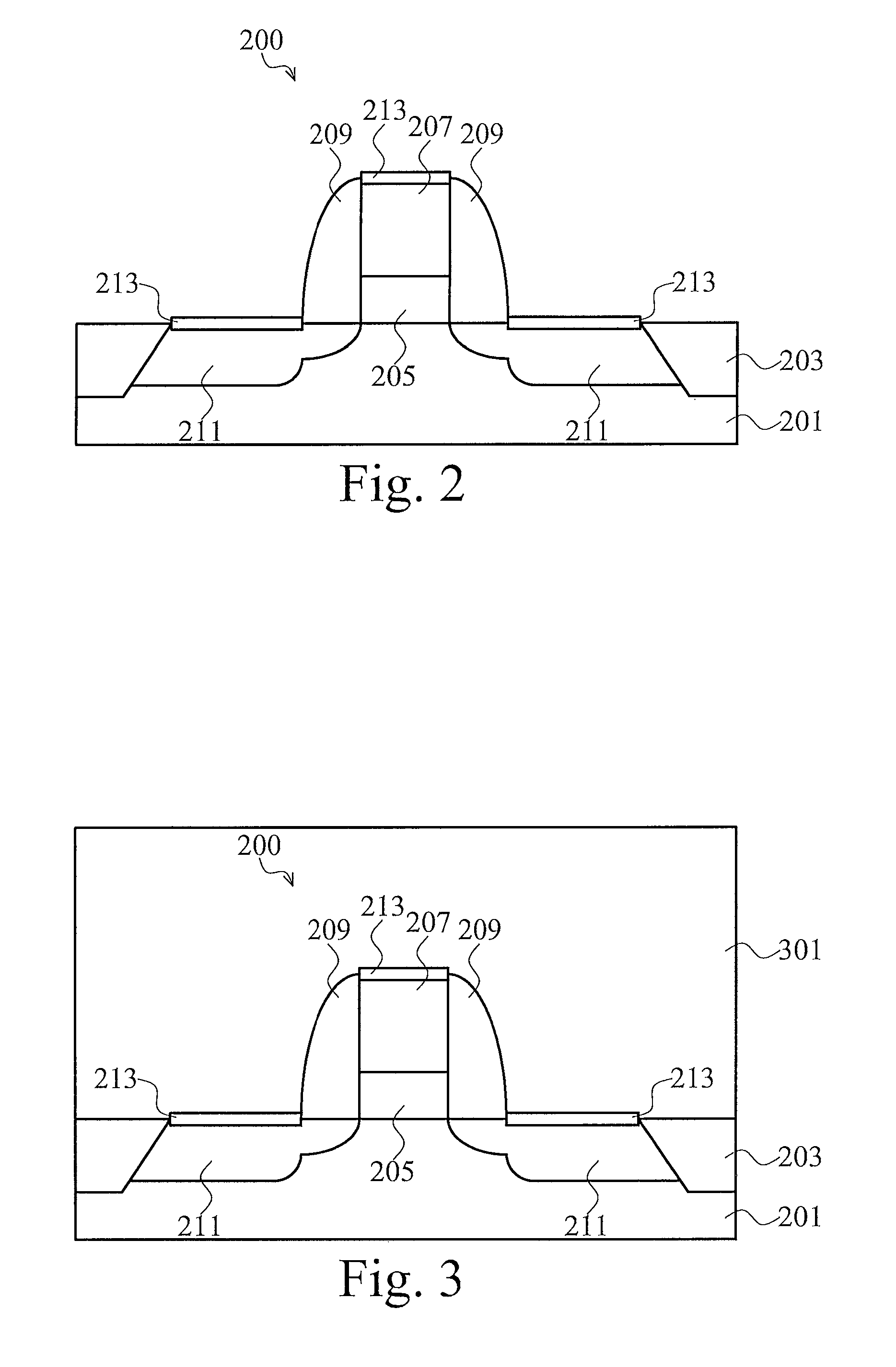
[0018]The present invention will be described with respect to forming a contact barrier layer to the source / drain regions of a field effect transistor. The invention may also be applied, however, to other contacts and vias such as those found through an interlayer dielectric layer.

[0019]With reference now to FIG. 2, there is shown a transistor 200 formed on a substrate 201 with shallow trench isolations (STIs) 203 formed therein. The transistor 200 generally comprises a gate dielectric 205, gate electrode 207, spacers 209, source / drain regions 211, and silicide contacts 213.

[...


PUM

PropertyMeasurementUnit
relative permittivityaaaaaaaaaa
thicknessaaaaaaaaaa

Abstract

System and method for reducing contact resistance and improving barrier properties is provided. An embodiment comprises a dielectric layer and contacts extending through the dielectric layer to connect to conductive regions. A contact barrier layer is formed between the conductive regions and the contacts by electroless plating the conductive regions after openings have been formed through the dielectric layer for the contact. The contact barrier layer is then treated to fill the grain boundary of the contact barrier layer, thereby improving the contact resistance. In another embodiment, the contact barrier layer is formed on the conductive regions by electroless plating prior to the formation of the dielectric layer.

Description

TECHNICAL FIELD[0001]The present invention relates generally to a system and method for forming electrical contacts and, more particularly, to a system and method for forming a barrier layer for electrical contacts.BACKGROUND[0002]In the race to improve transistor performance as well as to reduce the size of transistors, much research has been done on the contacts that connect a transistor's source and drain regions to the various layers of metallization over the transistor. In the search for better contacts, copper has been researched as a potential method to improve the resistance of the contact, as well as the overall performance of the device as a whole. However, the use of copper has some inherent problems that must be overcome, such as copper's propensity to migrate and cause unwanted reactions with other materials.[0003]FIG. 1 illustrates one attempt to overcome some of these problems of using copper as a contact. FIG. 1 illustrates a substrate 101 with shallow trench isolati...

Claims


Application Information

Patent Timeline
Patent Type & Authority Patents(United States)
IPC IPC(8): H01L21/44
CPCH01L21/28518H01L21/76843H01L21/76846H01L21/76856H01L29/665H01L29/7833H01L23/485
Inventor LIU, CHUNG-SHIYU, CHEN-HUA
Owner TAIWAN SEMICON MFG CO LTD
Why Eureka
Try Eureka