

Stacked-die package for battery power management
stacked die technology, applied in the direction of safety/protection circuit, emergency protection arrangement for limiting excess voltage/current, semiconductor/solid-state device details, etc., can solve the problems of reducing the efficiency of a power management package in this size range, limiting the space available for mosfets, and challenging conventional technology to further reduce the size of the battery protection integrated circuit (ic). , to achieve the effect of reducing the overall thickness of the package, reducing
- Summary
- Abstract
- Description
- Claims
- Application Information
AI Technical Summary
Benefits of technology
Problems solved by technology
Method used
Image

Examples
Embodiment Construction
[0023]Although the following detailed description contains many specific details for the purposes of illustration, anyone of ordinary skill in the art will appreciate that many variations and alterations to the following details are within the scope of the invention. Accordingly, the exemplary embodiments of the invention described below are set forth without any loss of generality to, and without imposing limitations upon, the claimed invention.
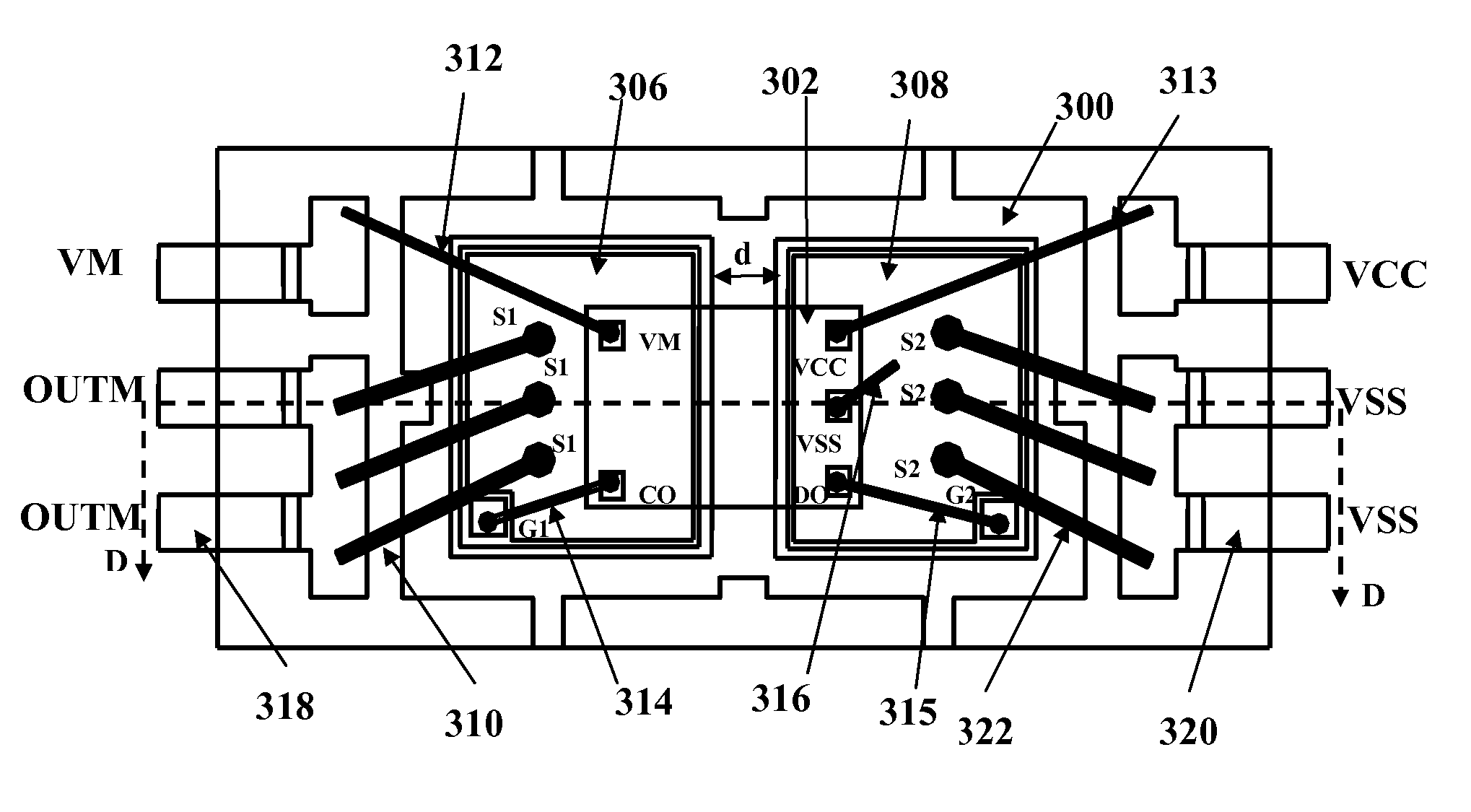
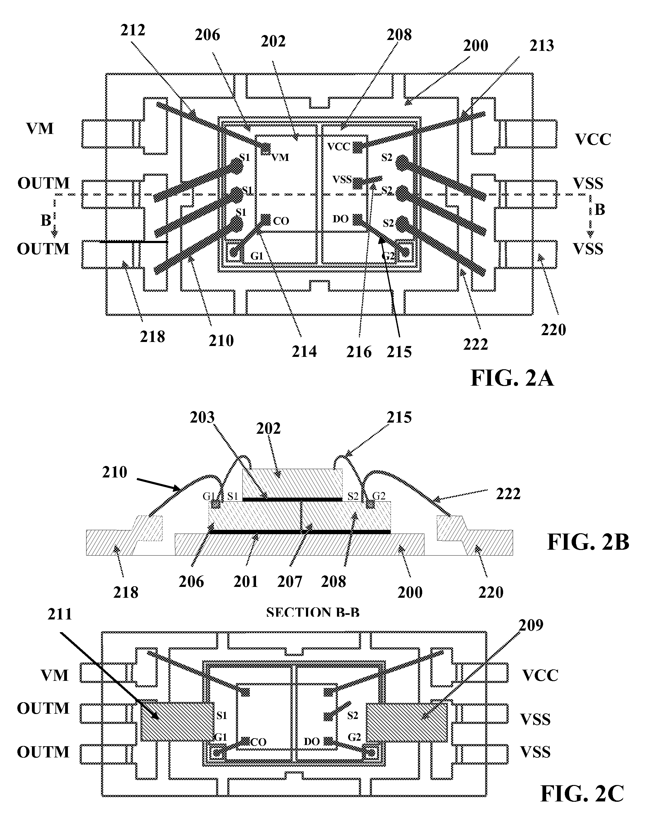
[0024]Embodiments of the present invention provide a battery protection package with better performance, smaller form factor and a superior pin-out arrangement. In embodiments of the present invention, a power control IC may be stacked on top of integrated dual common-drain MOSFETs or overlapping two discrete MOSFETs and single die pad may be utilized for attaching the MOSFETs of all configurations. FIG. 2A is a top view of a battery protection package assembly including integrated dual common-drain MOSFETs in which two MOSFETs of the equal ...
PUM
 Abstract
Description
Claims
Application Information