Supercharge Your Innovation With Domain-Expert AI Agents!

Bipolar transistor

a transistor and bipolar technology, applied in the field of bipolar transistors, can solve the problems of reducing the operating reducing the capacitance of the collector where the base contact is formed, and slowed down the contrariwise operation speed of the transistor, so as to reduce the capacitance, reduce the capacitance, and reduce the width of the emitter

Inactive Publication Date: 2011-04-12
JAPAN SCI & TECH CORP
View PDF18 Cites 3 Cited by
  • Summary
  • Abstract
  • Description
  • Claims
  • Application Information

AI Technical Summary

Benefits of technology

The present invention provides a bipolar transistor with a finer emitter, reduced parasitic capacitance between the collector and base, and improved high-frequency characteristics. The transistor has a subcollector layer, collector layer, base layer, and emitter layer. An insulator layer is formed on the base layer, and the insulator layer is opened in at least two portions to reduce the parasitic capacitance. The transistor has a reduced emitter width and a reduced base layer contact area, which reduces the base layer resistance and improves high-frequency performance. The manufacturing method of the transistor includes the steps of forming a collector contact layer, insulator layer, and extrinsic base layer. The width of the insulator layer is limited to reduce the parasitic capacitance and improve performance.

Problems solved by technology

If the emitter width is reduced to excess, however, the parasitic collector capacitance under the base where the base contact is formed becomes not negligible and the transistor contrariwise comes to be slowed down in operating speed.

Method used


Image

  • Bipolar transistor
  • Bipolar transistor
  • Bipolar transistor

Examples


example 1

Calculation Example 1

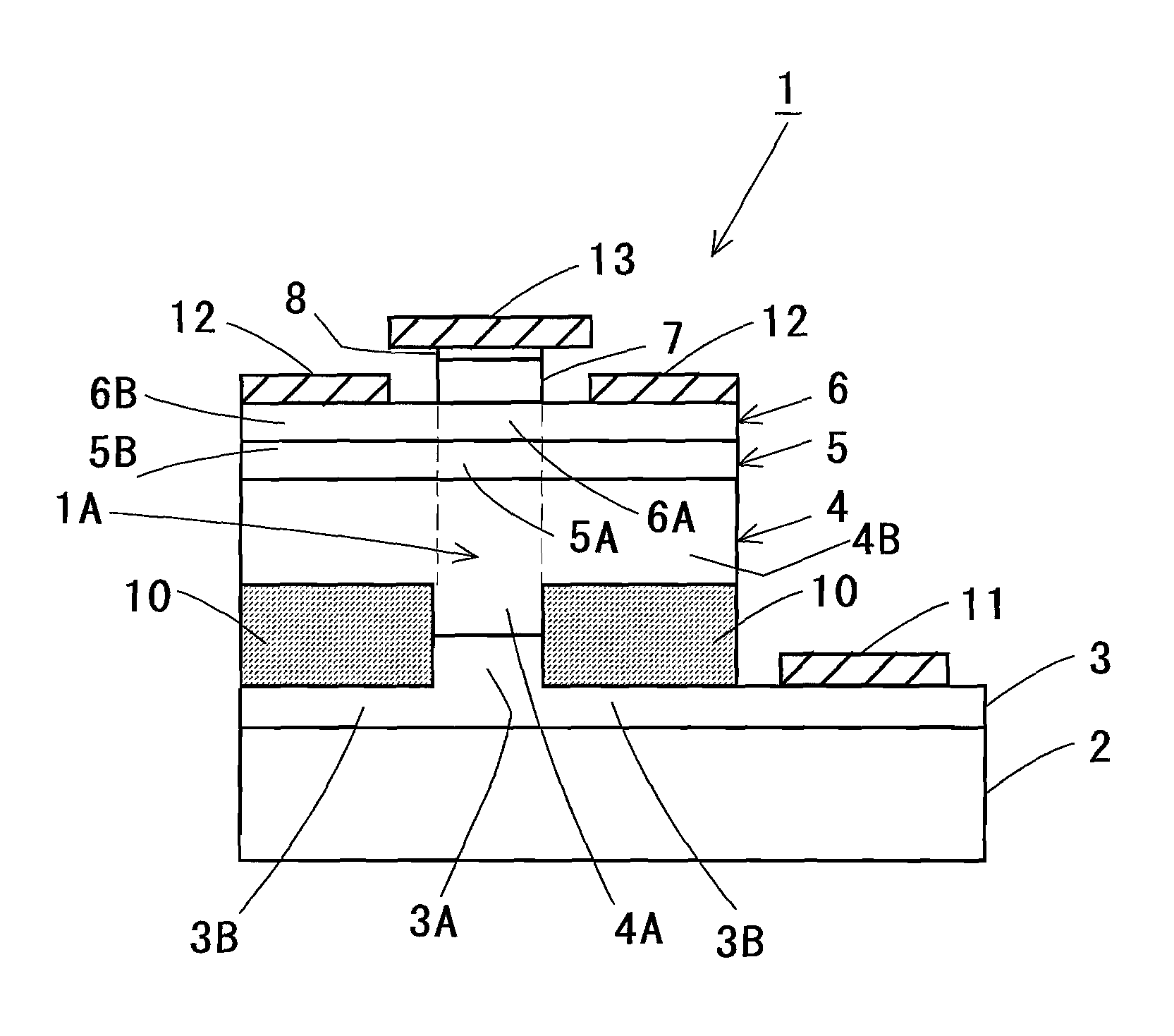
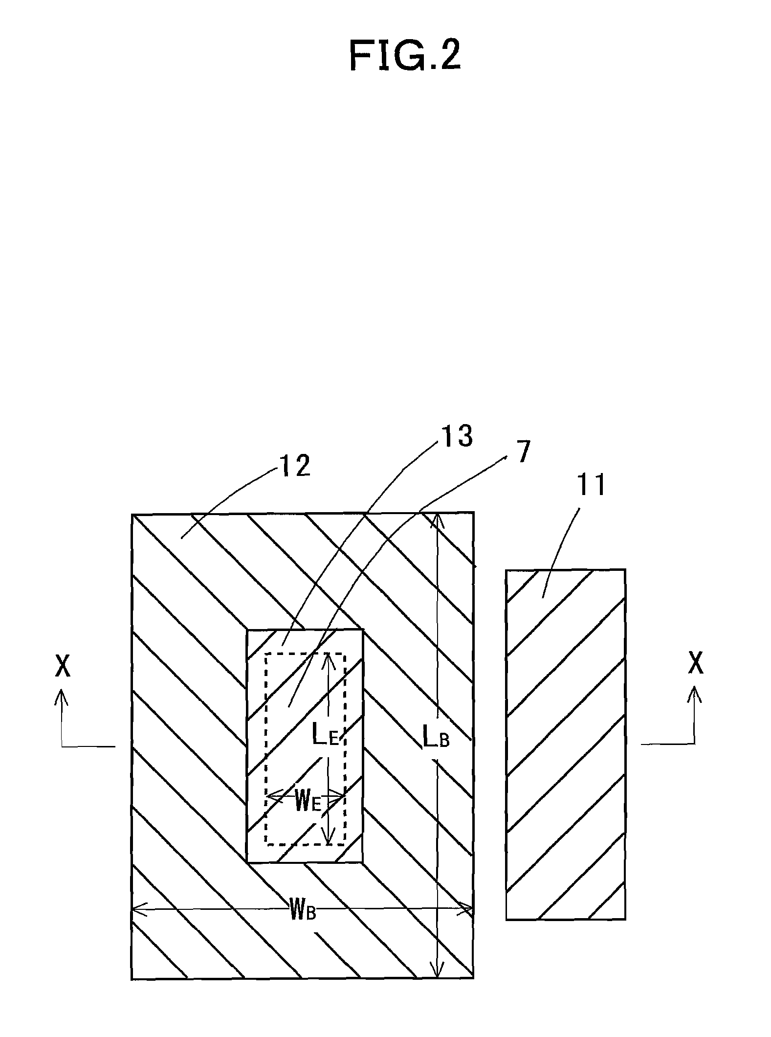
[0064]As the bipolar transistor 1 of the present invention, an InP heterojunction bipolar transistor 1, in which the semi-insulating substrate 2 was formed of InP, the subcollector layer 3 of two layers: n-type InP and InGaAs layers, the collector layers 4 and 5 of InP and InGaAs layers not incorporating any intentional impurity, the base layer 6 of InGaAs of p type, the emitter layer 7 of n type InP, and the contact layer 8 of n+ InGaAs, had various characteristics calculated with the parameters as follows:

[0065]size of emitter layer: emitter width WE=0.1 μm and emitter length LE=2 μm;

[0066]thickness of base layer: 30 nm;

[0067]thickness of collector layer: 150 nm;

[0068]size of insulator (SiO2) layer: width of 200 nm and height of 200 nm; and

[0069]dielectric constant of InP=12.4 and

[0070]dielectric constant of SiO2=3.9.

[0071]Using these parameters, the characteristics of the InP heterojunction bipolar transistor 1 were calculated as stated below.

[0072]That is: i...

example

[0090]Mention is made of the present invention in further detail in respect to a specific example thereof as follows:

[0091]As an Example, a heterojunction bipolar transistor of InP was prepared.

[0092]First, a subcollector layer 3 of 600 nm thickness was formed on a semi-insulating substrate 2 of InP using the metalorganic vapor-phase epitaxy.

[0093]Next, a SiO2 film of 60 nm thickness was deposited on the whole surface by the plasma assisted CVD method and after an electron beam resist film was applied thereto, only areas of 140 nm width where thin wires are to be formed becoming the insulator layer are exposed. The wire forming areas are longitudinally oriented in crystallographic direction with respect to the substrate surface in (100) plane of the InP semi-insulating substrate 2.

[0094]Next, by the so-called lift-off process, namely by: upon vapor deposition of a thin film of aluminum entirely on the electron beam resist film with the wire forming areas opened, removing the electr...


PUM


Abstract

A bipolar transistor (1) comprising a subcollector layer (3), a collector layer (4, 5), a base layer (6) and an emitter layer (7) which are successively built up and having: the subcollector layer (3) formed with a projection (3A) and recesses (3B), an upper part above the projection constituting an intrinsic transistor region (1A) of the bipolar transistor; insulator layer (10) buried between the recesses of the subcollector layer and the collector layer (4); a boundary interface between the subcollector layer and the collector layer held between the insulator layers; the base layer (6) made of a single crystal layer and provided with a base electrode (12) on a region becoming an extrinsic base layer (6B) of the base layer; and the subcollector layer provided with a collector electrode (11). The bipolar transistor has advantages of its emitter made finer in width, a reduced parasitic capacitance between its base and collector and improved high-frequency characteristics.

Description

TECHNICAL FIELD[0001]The present invention relates to a bipolar transistor and a manufacturing method of the same and in particular to a bipolar transistor having its emitter that can be made finer in width, a reduced parasitic capacitance created between its collector and base layer and improved high-frequency characteristics, and a manufacturing method the same.BACKGROUND ART[0002]A bipolar transistor is formed by fabricating a multilayer structure having a subcollector layer, a collector layer, a base layer and an emitter layer deposited in order and then providing electrodes for the emitter, base and subcollector layers, respectively. While an InP heterojunction bipolar transistor is a fast transistor whose cut-off frequency has been reported to be currently the highest, its fastness depends on increasing the current density by reduction of its size and shortening its transit time. If the emitter width is reduced to excess, however, the parasitic collector capacitance under the ...

Claims


Application Information

Patent Timeline
Patent Type & Authority Patents(United States)
IPC IPC(8): H01L21/331
CPCH01L29/7371H01L29/66318H01L29/20
Inventor MIYAMOTO, YASUYUKIYAMAMOTO, TOHRUISHIDA, MASASHI
Owner JAPAN SCI & TECH CORP
Features
  • R&D
  • Intellectual Property
  • Life Sciences
  • Materials
  • Tech Scout
  • Unparalleled Data Quality
  • Higher Quality Content
  • 60% Fewer Hallucinations
Learn More