Integrated millimeter wave antenna and transceiver on a substrate

a technology of integrated millimeter wave antenna and substrate, which is applied in the direction of resonant antenna, antenna equipment with additional functions, and protection material radiating elements, etc., can solve the problems of difficult to provide structural integrity, mismatch impedance at the interface between the antenna and the semiconductor chip, and the difficulty of capturing millimeter wave signals, so as to improve the radiation efficiency of the antenna, reduce the effective dielectric constant, and reduce the wavelength of the millimeter wave

Active Publication Date: 2011-05-17
GLOBALFOUNDRIES US INC
View PDF10 Cites 19 Cited by
  • Summary
  • Abstract
  • Description
  • Claims
  • Application Information

AI Technical Summary

Benefits of technology

[0012]In the present invention, a semiconductor chip integrating a transceiver, an antenna, and a receiver is provided. The transceiver is formed on a front side of a semiconductor substrate. At least one through substrate via provides electrical connection between the transceiver and the backside of the semiconductor substrate. The antenna, which is connected to the transceiver, is formed in a dielectric layer on the front side of the substrate. The reflector plate is connected to the through substrate via, and is formed on the backside of the semiconductor substrate. The separation between the reflector plate and the antenna is about a quarter wavelength of millimeter waves, which enhances radiation efficiency of the antenna. An array of through substrate trenches may be formed and filled with a dielectric material to reduce the effective dielectric constant of the material between the antenna and the reflector plate, thereby reducing the wavelength of the millimeter wave and enhance the radiation efficiency.

Problems solved by technology

The capture of millimeter wave signals poses a unique difficulty due to the short wavelength of the millimeter wave signals.
Prior efforts to attach a millimeter wave antenna to a semiconductor chip through a C4 pad or a wirebond pad have resulted in mismatched impedance at the interface between the antenna and the semiconductor chip, which is typically the C4 ball or the wirebond pad.
Further, aligning a reflector plate, which is necessary to increase efficiency of the antenna, to the semiconductor chip and the antenna to provide structural integrity is a challenging task.
Incorporation of a millimeter wave antenna into a wiring level dielectric material layer on a semiconductor chip has resulted in poor performance since the distance between the antenna and the reflector plate needs to about the quarter wavelength of the millimeter wave, which is in the range of hundreds of microns, and the total thickness of a metal wiring structure in conventional semiconductor chips is from several microns to about 20 microns.
Without a sufficient volume to incorporate a functional reflector plate, any prior art integrated antenna in a semiconductor chip displays poor signal capture efficiency, rendering such an antenna inefficient.

Method used


Image

  • Integrated millimeter wave antenna and transceiver on a substrate
  • Integrated millimeter wave antenna and transceiver on a substrate
  • Integrated millimeter wave antenna and transceiver on a substrate

Examples


Embodiment Construction

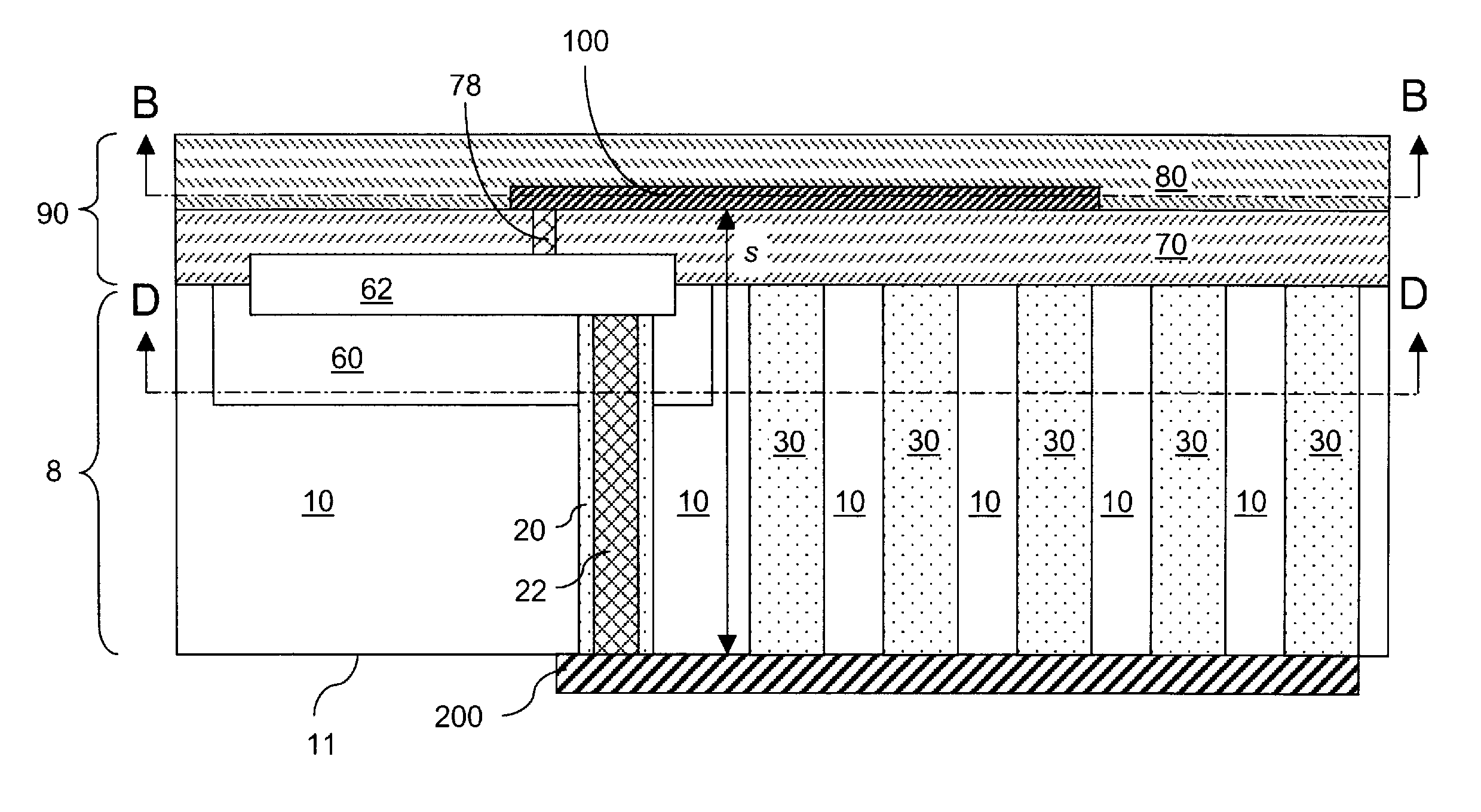
[0042]As stated above, the present invention relates to a semiconductor structure including an integrated millimeter wave antenna, a reflector plate, and a transceiver on a substrate, and methods of forming the same. As used herein, when introducing elements of the present invention or the preferred embodiments thereof, the articles “a”, “an”, “the” and “said” are intended to mean that there are one or more of the elements. Throughout the drawings, the same reference numerals or letters are used to designate like or equivalent elements. Detailed descriptions of known functions and constructions unnecessarily obscuring the subject matter of the present invention have been omitted for clarity. The drawings are not necessarily drawn to scale.

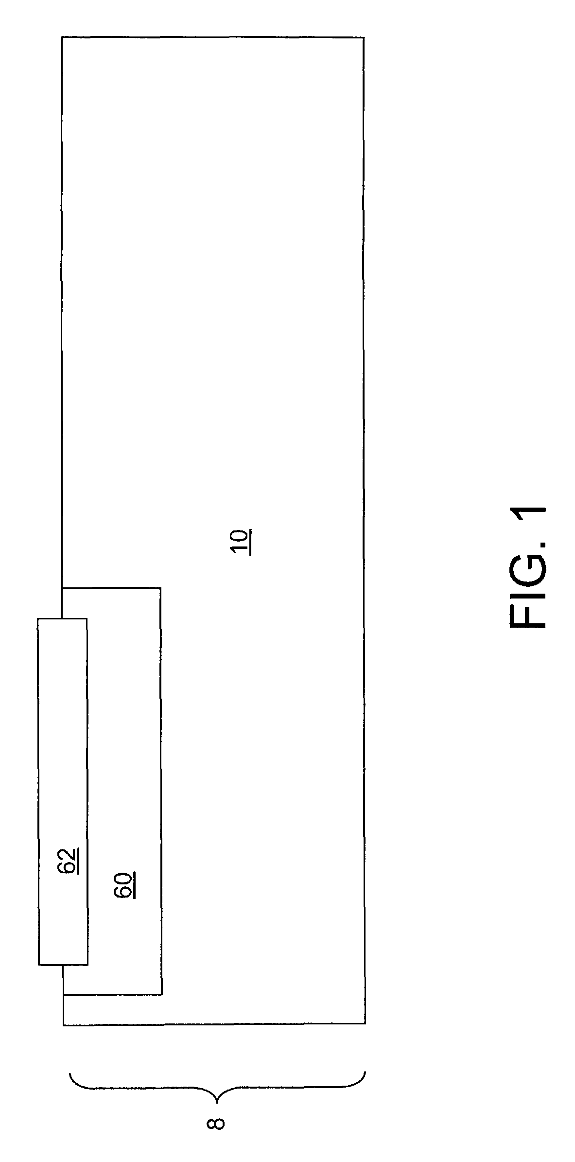
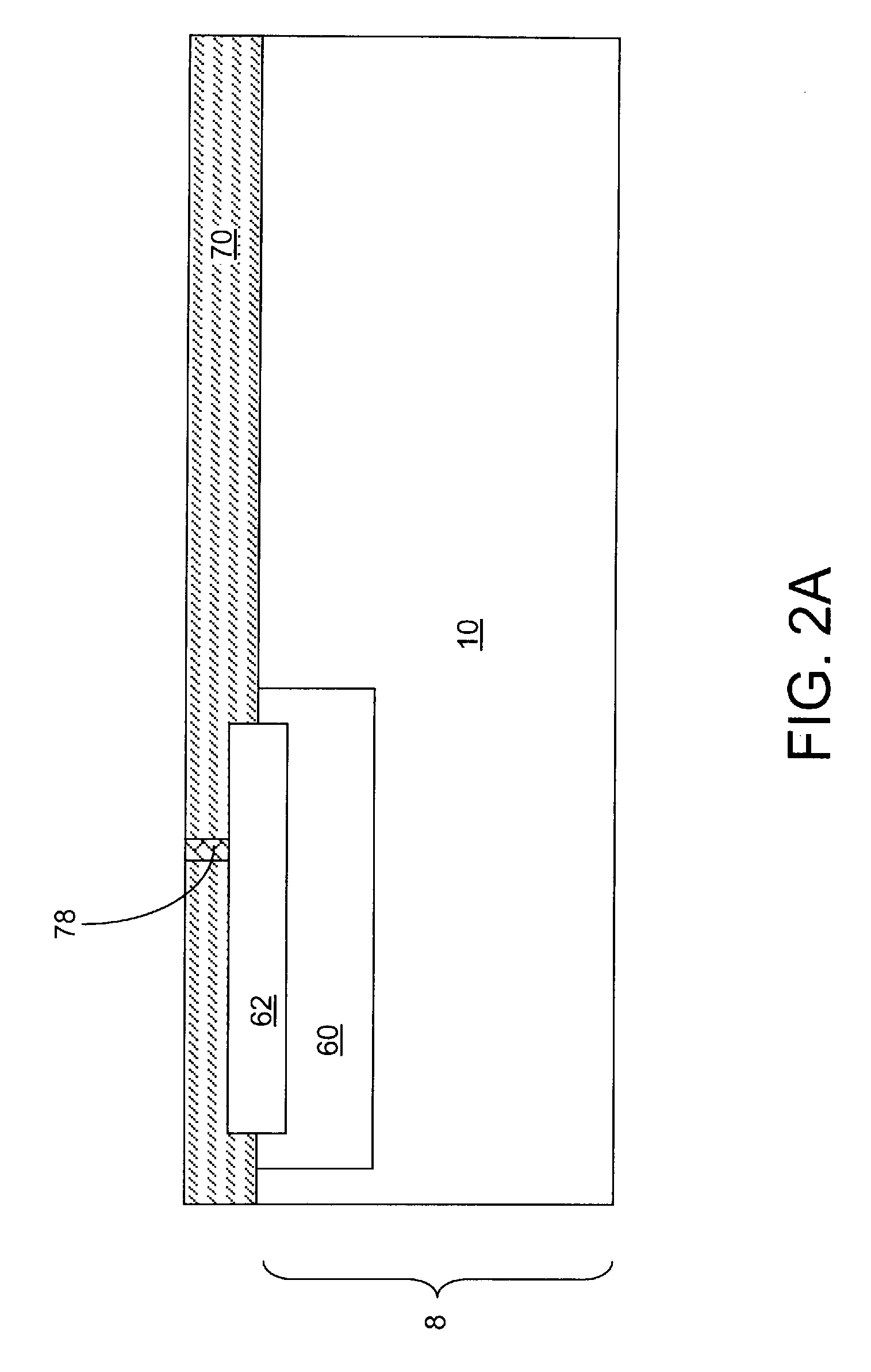
[0043]Referring to FIG. 1, a first exemplary semiconductor structure according to a first embodiment of the present invention comprises a semiconductor substrate 8, which includes a high resistivity semiconductor portion 10 and a low resistivity se...


PUM


Abstract

A semiconductor chip integrating a transceiver, an antenna, and a receiver is provided. The transceiver is formed on a front side of a semiconductor substrate. At least one through substrate via provides electrical connection between the transceiver and the backside of the semiconductor substrate. The antenna, which is connected to the transceiver, is formed in a dielectric layer on the front side. The reflector plate is connected to the through substrate via, and is formed on the backside. The separation between the reflector plate and the antenna is about the quarter wavelength of millimeter waves, which enhances radiation efficiency of the antenna. An array of through substrate trenches may be formed and filled with a dielectric material to reduce the effective dielectric constant of the material between the antenna and the reflector plate, thereby reducing the wavelength of the millimeter wave and enhance the radiation efficiency.

Description

RELATED APPLICATIONS[0001]The present application is related to co-pending U.S. application Ser. No. 12 / 187,442, which is incorporated herein by reference.FIELD OF THE INVENTION[0002]The present invention relates to semiconductor structures, and particularly to a semiconductor structure including an integrated millimeter wave antenna, a reflector plate, and a transceiver on a substrate, and methods of forming the same.BACKGROUND OF THE INVENTION[0003]Millimeter waves refer to electromagnetic radiation having a wavelength range from about 1 mm to about 10 mm. The corresponding frequency range for millimeter waves is from about 30 GHz to about 300 GHz. The wavelength range for the millimeter waves occupies the highest frequency range for microwaves, and is also referred to as extremely high frequency (EHF). The frequency range for the millimeter waves is the highest radio frequency band, and the electromagnetic radiation having a higher frequency than the millimeter waves is considere...

Claims


Application Information

Patent Timeline
Patent Type & Authority Patents(United States)
IPC IPC(8): H01L21/00
CPCH01Q9/28H01Q1/40
Inventor DING, HANYIFENG, KAI D.HE, ZHONG-XIANGJIN, ZHENRONGLIU, XUEFENG
Owner GLOBALFOUNDRIES US INC
Why Eureka
Try Eureka