In-situ process layer using silicon-rich-oxide for etch selectivity in high AR gapfill

a technology of silicon-rich-oxide and process layer, which is applied in the direction of chemical vapor deposition coating, metallic material coating process, coating, etc., can solve the problem that the etching of reactive plasma may not be fully isotropic, and achieve the effect of reducing the incidence of voids or weak spots

Active Publication Date: 2011-05-31
NOVELLUS SYSTEMS
View PDF20 Cites 36 Cited by
  • Summary
  • Abstract
  • Description
  • Claims
  • Application Information

AI Technical Summary

Benefits of technology

[0011]The present invention addresses this need by providing high density plasma chemical vapor deposition (HDP CVD) of a dielectric layer, followed by HDP chemical vapor deposition of an etch selectivity layer, and subsequently providing an etch back process. This multi-step process can be repeated as necessary to fill high aspect ratio (typically at least 6:1, for example 7:1 or higher), narrow width (typically sub 0.13 micron, for example 0.1 micron or less) gaps with significantly reduced incidence of voids or weak spots.
[0013]The etch back part of the process involves both sputter etching and reactive plasma etching. A sputter etch may apply bias to the substrate pedestal to induce ion bombardment at the substrate surface for a period of about 10-150 seconds, for example about 60 seconds, depending on the source and bias powers used for different sputter chemistries. The sputtering gas may comprise hydrogen, deuterium, helium, nitrogen, argon, or a combination of these. The sputter etching can reduce the size of top hats adjacent to a gap opening without completely opening the gap.

Problems solved by technology

If bias is used, then the reactive plasma etch may not be fully isotropic.

Method used


Image

  • In-situ process layer using silicon-rich-oxide for etch selectivity in high AR gapfill
  • In-situ process layer using silicon-rich-oxide for etch selectivity in high AR gapfill
  • In-situ process layer using silicon-rich-oxide for etch selectivity in high AR gapfill

Examples


example

[0114]The following example is provided to illustrate certain aspects of the present invention. The example will serve to further illustrate the invention but is not meant to limit the scope of the invention in any way.

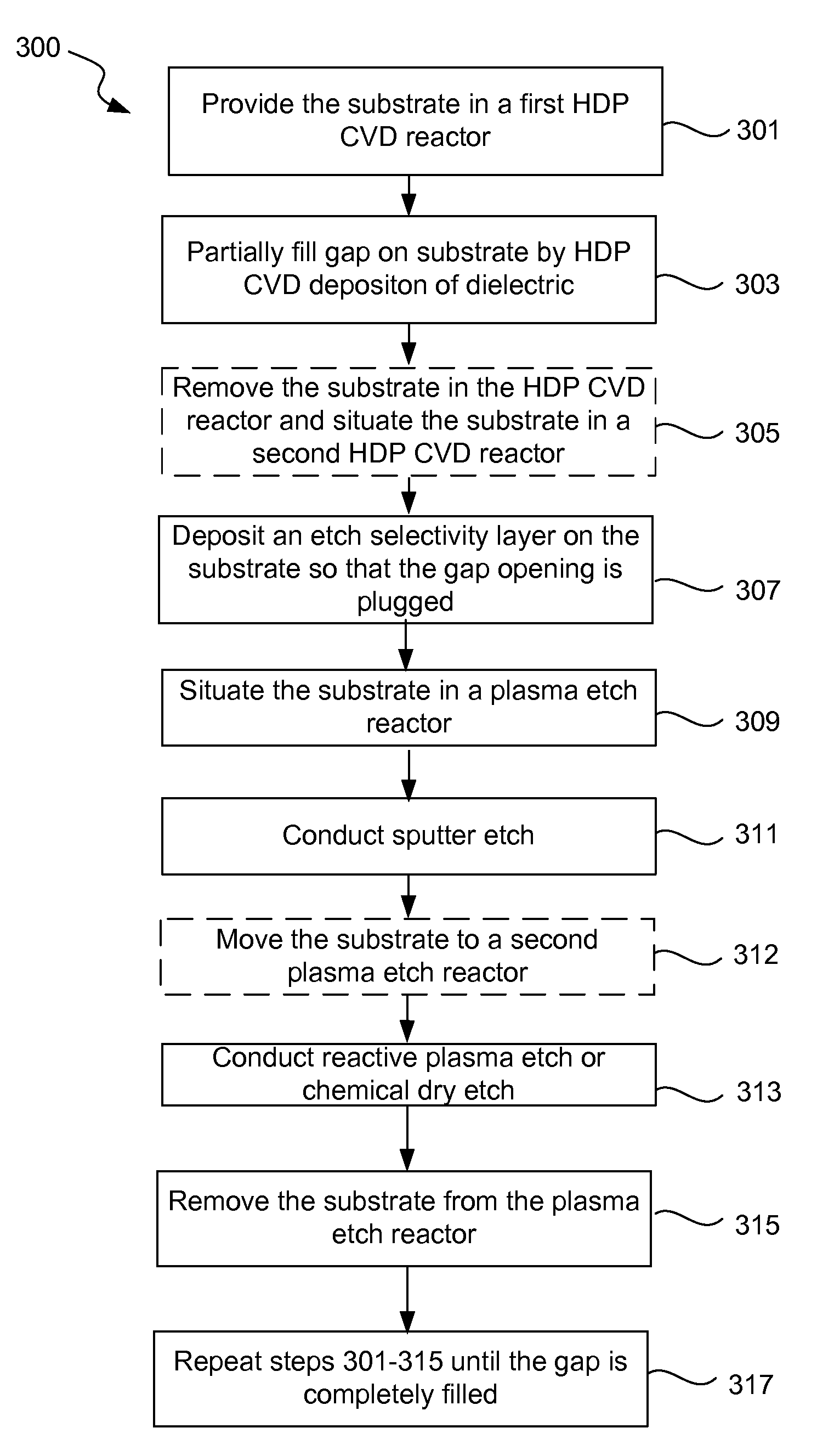
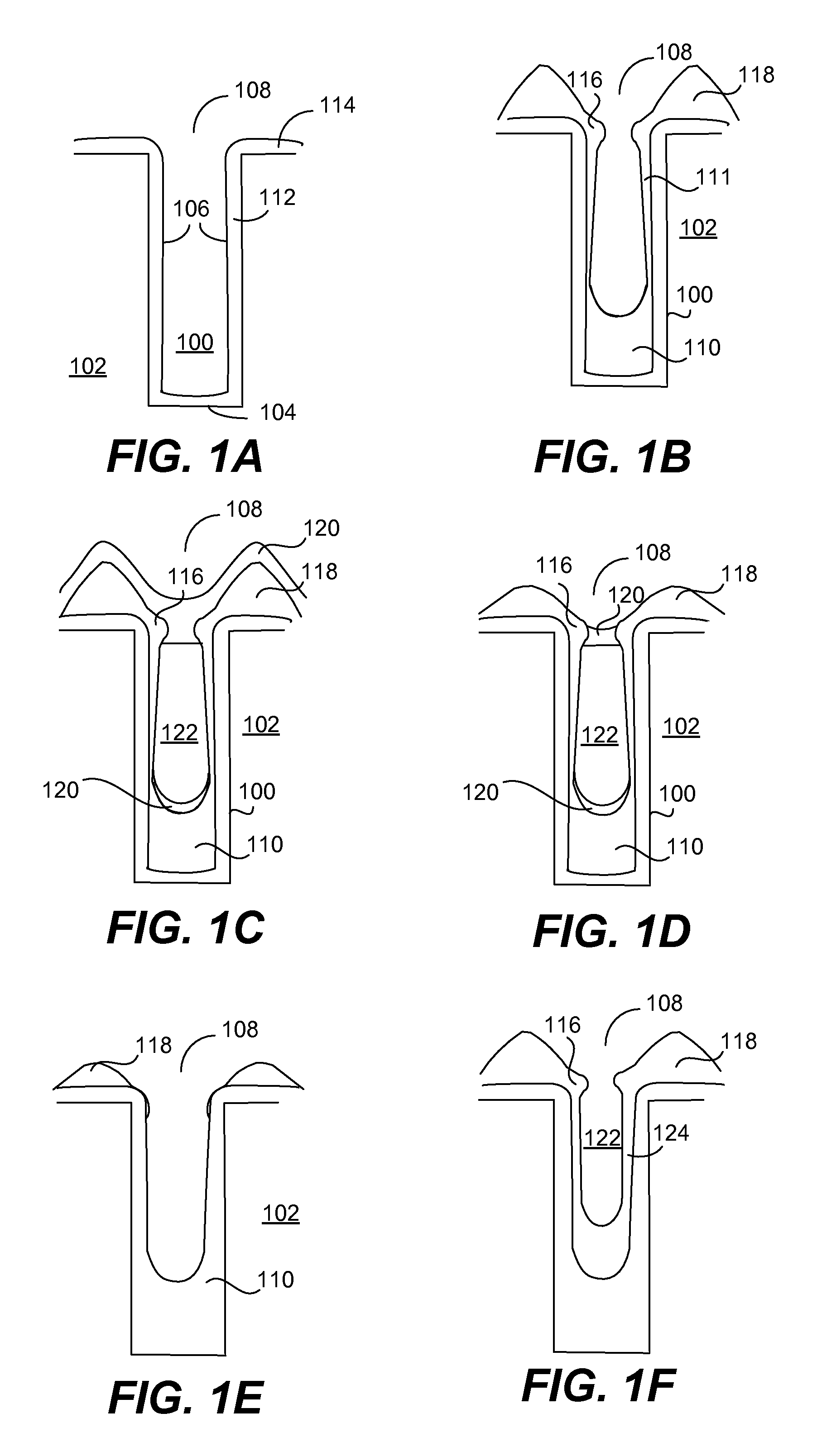
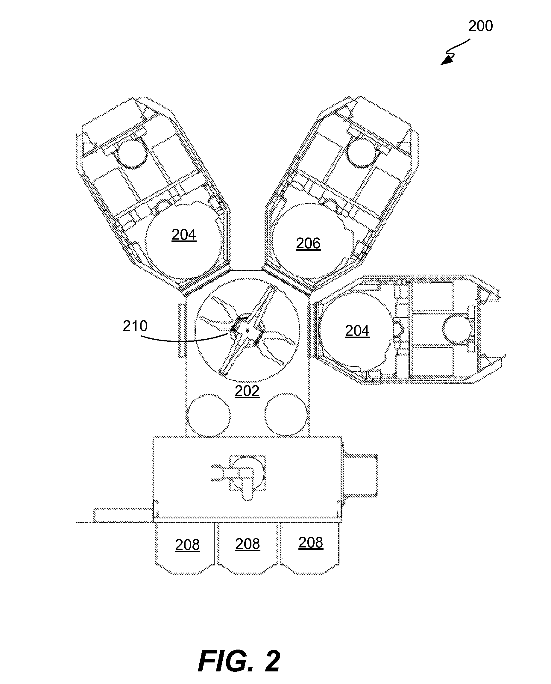
[0115]In this example, one embodiment of the methods discussed herein was practiced on a SPEED semiconductor processing tool from Novellus Systems. First a layer of dielectric was deposited using an HDP CVD reactor onto multiple substrates having gaps. The thickness of the bottom fill, the top hat, and the sidewalls were measured and plotted in FIG. 4 as “Dep.” After the initial deposition, the bottom thickness was about 980 angstroms; the top hat, about 1250 angstroms; and the sidewall, about 177 angstroms. The aspect ratio of the remaining gap was measured and shown in FIG. 5. After the initial deposition, the aspect ratio was about 7.8.

[0116]After the initial deposition, an SRO etch selectivity layer was deposited onto one of the substrates. The SRO was deposited o...


PUM

PropertyMeasurementUnit
thicknessaaaaaaaaaa
thicknessaaaaaaaaaa
pressuresaaaaaaaaaa

Abstract

In-situ semiconductor process that can fill high aspect ratio (typically at least 6:1, for example 7:1 or higher), narrow width (typically sub 0.13 micron, for example 0.1 micron or less) gaps with significantly reduced incidence of voids or weak spots is provided. This deposition part of the process may involve the use of any suitable high density plasma chemical vapor deposition (HDP CVD) chemistry. Prior to etch back, the feature gap is plugged with an etch selectivity layer. The etch back part of the process involves multiple steps including a sputter etch to reduce the top hat formations followed by a reactive plasma etch to open the gap. This method improves gapfill, reduces the use of high cost fluorine-based etching and produces interim gaps with better sidewall profiles and aspect ratios.

Description

FIELD OF THE INVENTION[0001]This invention relates to electronic device fabrication processes and associated apparatus. More specifically, the invention relates to chemical vapor deposition and dry etch processes for forming dielectric layers, particularly in high aspect ratio, narrow width recessed features.BACKGROUND OF THE INVENTION[0002]It is often necessary in semiconductor processing to fill high aspect ratio gaps with insulating material. This is the case for shallow trench isolation, inter-metal dielectric layers, pre-metal dielectric layers, passivation layers, etc. As device geometries shrink and thermal budgets are reduced, void-free filling of narrow width, high aspect ratio spaces (e.g., AR>3:1, and particularly AR>6:1) becomes increasingly difficult due to limitations of existing deposition processes.[0003]High density plasma (HDP) chemical vapor deposition (CVD), a directional (bottom-up) CVD process, is the method currently used for high aspect ratio gapfill. H...

Claims


Application Information

Patent Timeline
Patent Type & Authority Patents(United States)
IPC IPC(8): H01L21/76
CPCC23C16/045C23C16/402H01L21/02126H01L21/02129H01L21/02131H01L21/02164H01L21/76837H01L21/31055H01L21/31056H01L21/31105H01L21/31116H01L21/76224H01L21/02274
Inventor SHANKER, SUNIL
Owner NOVELLUS SYSTEMS
Why Eureka
Try Eureka