Photoelectric conversion device and solid-state imaging device

a conversion device and photoelectric technology, applied in the direction of picture signal generators, television systems, radio control devices, etc., can solve the problems of reducing the efficiency of photoelectric conversion, limiting the thickness of the photoelectric conversion layer, and lowering the sensitivity of the device, so as to prevent the sensitivity lowering and broaden the spectral sensitivity

Active Publication Date: 2011-05-31
FUJIFILM CORP +1
View PDF47 Cites 9 Cited by
  • Summary
  • Abstract
  • Description
  • Claims
  • Application Information

AI Technical Summary

Benefits of technology

[0006]In the photoelectric conversion layer made of an organic material, it is general that in the foregoing configuration, when light is made incident from the upper part of the second electrode layer, an electron and a hole are generated in large amounts in the vicinity of the second electrode layer due to the light absorption, whereas an electron and a hole are not generated in such large amounts in the vicinity of the first electrode layer. This is caused due to the matter that a major part of light in the vicinity of the absorption peak wavelength of this photoelectric conversion layer is absorbed in the vicinity of the second electrode layer and that when it becomes more distant from the vicinity of the second electrode layer, an absorptance of light is lowered. For that reason, so far as an electron or a hole as generated in the vicinity of the second electrode layer does not efficiently transfer into the silicon substrate, the photoelectric conversion efficiency is lowered, resulting in a lowering of the sensitivity of the device. Also, a signal due to the light wavelength as strongly absorbed in the vicinity of the second electrode layer is reduced, resulting in so-called broadening such that the width of the spectral sensitivity is widened.
[0007]Also, in the photoelectric conversion layer made of an organic material, it is general that the mobility of the electron is very small as compared with that of the hole. In addition, in the photoelectric conversion layer made of an organic material, it is known that the mobility of the electron is likely influenced by oxygen and that when the photoelectric conversion layer is exposed in the air, the mobility of the electron is further lowered. For that reason, in the case where it is intended to transfer the electron into the silicon substrate, if the transfer distance of the electron as generated in the vicinity of the second electrode layer within the photoelectric conversion layer is long, the electron is not collected by the electrode layer by, for example, the matter that a part of the electron is deactivated during the transfer, resulting in a lowering of the sensitivity and broadening of the spectral sensitivity.
[0009]For the purpose of preventing a lowering of the sensitivity and broadening of the spectral sensitivity from occurring, it is effective to efficiently transfer an electron or a hole as generated in the vicinity of the second electrode layer into a charge storage / transfer / read-out (silicon) substrate. In order to realize this, how to treat an electron or a hole as generated within the photoelectric conversion layer is a problem.
[0034]According to the invention, it is possible to provide a photoelectric conversion device which is able to prevent a lowering of the sensitivity and broadening of the spectral sensitivity from occurring.

Problems solved by technology

For that reason, so far as an electron or a hole as generated in the vicinity of the second electrode layer does not efficiently transfer into the silicon substrate, the photoelectric conversion efficiency is lowered, resulting in a lowering of the sensitivity of the device.
However, since it is necessary to obtain a sufficient amount of the light absorption, there is a limit in making the thickness of the photoelectric conversion layer thin; and if it is intended to meet the requirements regarding the mobility, there is a demerit that the material is largely limited.
However, in the case of applying a sufficiently strong electric field, there is some possibility of causing a lowering of S / N of a sensor such as an increase of an injective leak current from the two electrodes interposing the photoelectric conversion layer therebetween.
In order to realize this, how to treat an electron or a hole as generated within the photoelectric conversion layer is a problem.

Method used


Image

  • Photoelectric conversion device and solid-state imaging device
  • Photoelectric conversion device and solid-state imaging device
  • Photoelectric conversion device and solid-state imaging device

Examples


first embodiment

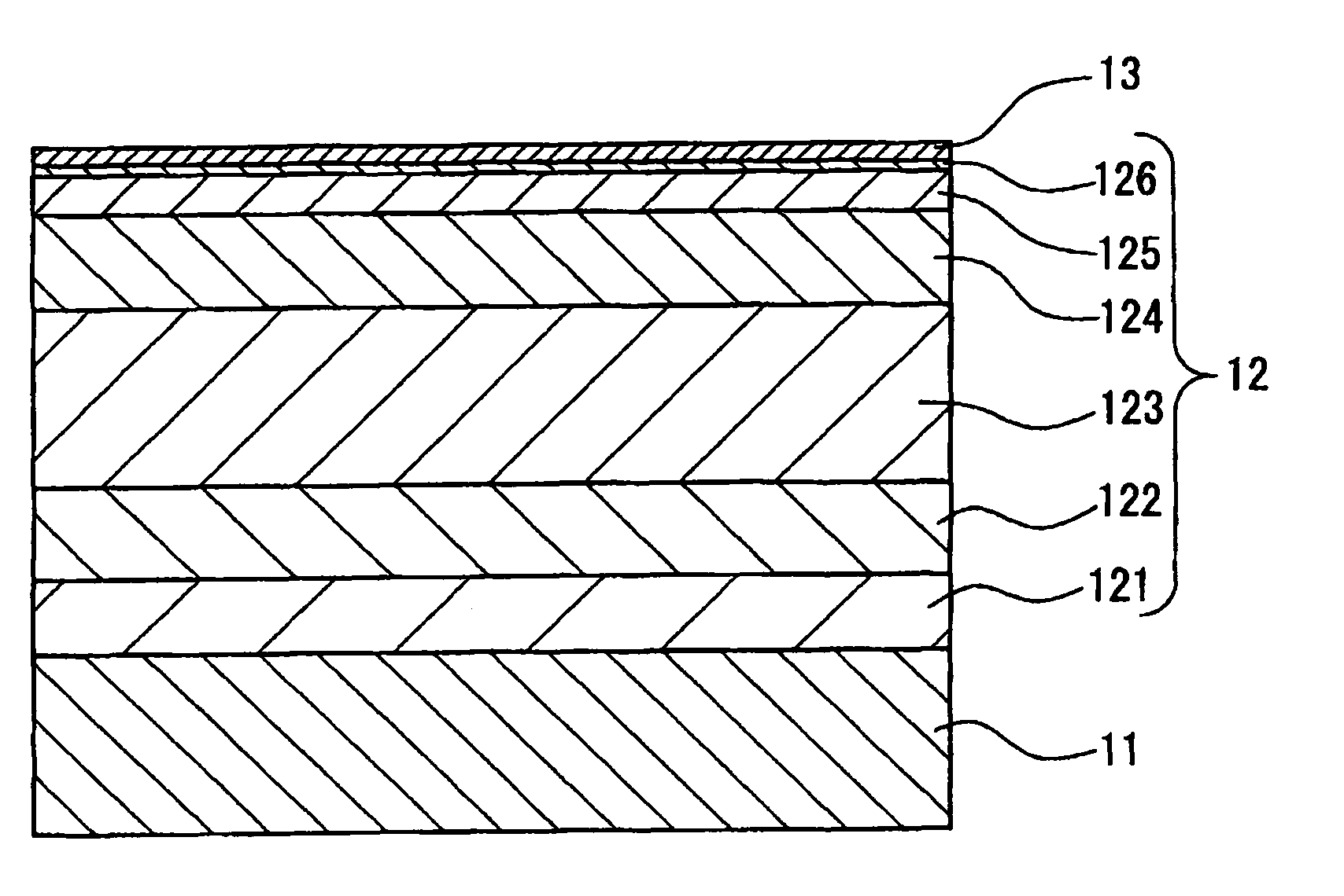
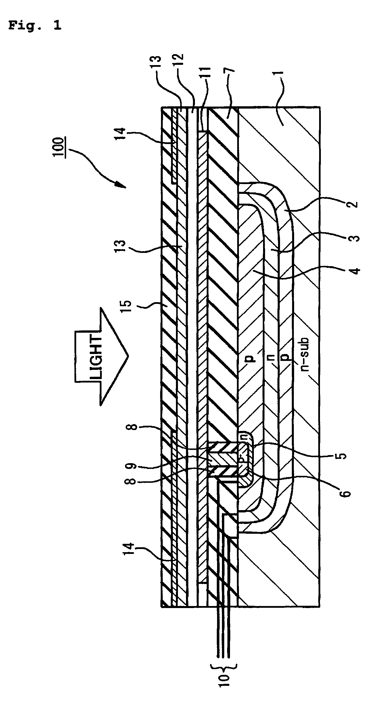
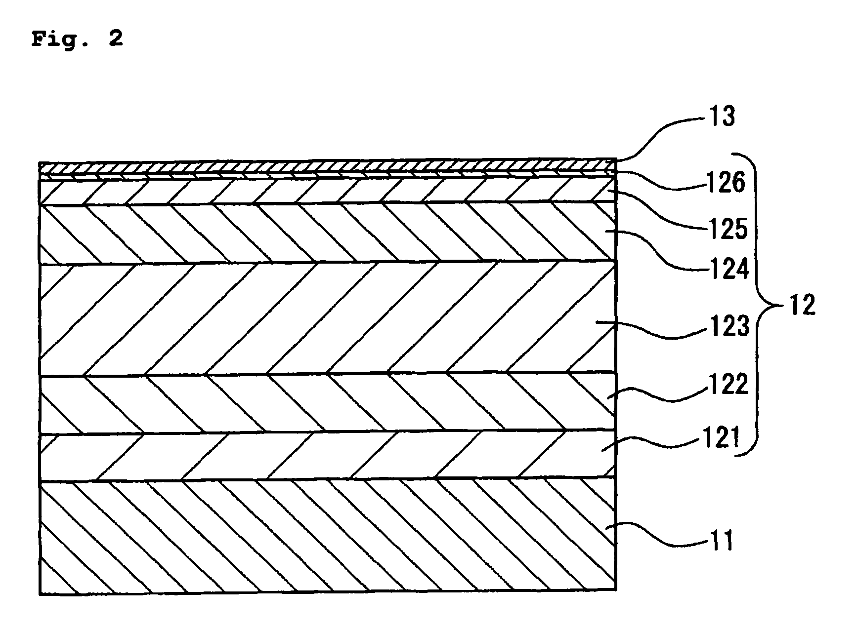
[0047]FIG. 1 is a cross-sectional schematic view of a portion of one pixel of a solid-state imaging device for explaining a first embodiment of the invention. FIG. 2 is a cross-sectional schematic view of a photoelectric conversion layer as illustrated in FIG. 1. In this solid-state imaging device, a plural number of the one pixel as illustrated in FIG. 1 is disposed in an array state on the same plane, and one pixel data of image data can be produced by a signal as obtained from this one pixel.

[0048]One pixel of a solid-state imaging device 100 as illustrated in FIG. 1 is configured to contain a photoelectric conversion part which is made of an n-type silicon substrate 1, a transparent insulating layer 7 as formed on the n-type silicon substrate 1, a first electrode layer 11 as formed on the insulating layer 7, a photoelectric conversion layer 12 as formed on the first electrode layer 11, and a second electrode layer 13 as formed on the photoelectric conversion layer 12; a light-sh...

second embodiment

[0113]In this embodiment, the inorganic layer having a configuration as illustrated in FIG. 1 which is described in the first embodiment is prepared in such a manner that two photodiodes are not stacked within the n-type silicon substrate but that two photodiodes are arranged in a direction vertical to an incident direction of the incident light, thereby detecting lights of two colors within the n-type silicon substrate.

[0114]FIG. 3 is a cross-sectional schematic view of a portion of one pixel of a solid-state imaging device for explaining a second embodiment of the invention.

[0115]One pixel of a solid-state imaging device 200 as illustrated in FIG. 3 is configured to contain a photoelectric conversion part which is made of an n-type silicon substrate 17, a first electrode layer 30 as formed in an upper part of the n-type silicon substrate 17, a photoelectric conversion layer 31 as formed on the first electrode layer 30, and a second electrode layer 32 as formed on the photoelectric...

third embodiment

[0127]A solid-state imaging device of this embodiment is configured such that the inorganic layer having a configuration as illustrated in FIG. 1 which is described in the first embodiment is not provided and plural (three in this instance) photoelectric conversion layers are stacked in an upper part of the silicon substrate.

[0128]FIG. 4 is a cross-sectional schematic view of a portion of one pixel of a solid-state imaging device for explaining a third embodiment of the invention.

[0129]A solid-state imaging device 300 as illustrated in FIG. 4 is configured such that an R photoelectric conversion part containing a first electrode layer 56, a photoelectric conversion layer 57 as stacked on the first electrode layer 56 and a second electrode layer 58 as stacked on the photoelectric conversion layer 57; a B photoelectric conversion part containing a first electrode layer 60, a photoelectric conversion layer 61 as stacked on the first electrode layer 60 and a second electrode layer 62 as...


PUM

PropertyMeasurementUnit
work functionaaaaaaaaaa
light transmittanceaaaaaaaaaa
angleaaaaaaaaaa

Abstract

A photoelectric conversion device comprising a photo-electric conversion part including a first electrode layer, a second electrode layer and a photoelectric conversion layer provided between the first electrode layer and the second electrode layer, wherein light is made incident from an upper part of the second electrode layer into the photoelectric conversion layer; the photoelectric conversion layer generates a charge containing an electron and a hole corresponding to the incident light from the upper part of the second electrode layer; and the first electrode layer works as an electrode for extracting the hole.

Description

FIELD OF THE INVENTION[0001]The present invention relates to a photoelectric conversion device including a photoelectric conversion part containing a first electrode layer, a second electrode layer opposing to the first electrode layer and a photoelectric conversion layer disposed between the first electrode layer and the second electrode layer and to a solid-state imaging device in which a plural number of this photoelectric conversion device is disposed in an array state.BACKGROUND OF THE INVENTION[0002]With respect to optical sensors of the related art, a device which is prepared by forming a photodiode (PD) in a semiconductor substrate such as silicon (Si) is general. As a solid-state imaging device, there is widely employed a planar solid-state imaging device in which PDs are two-dimensionally arranged in a semiconductor substrate and a signal corresponding to a signal charge as generated from each PD by photoelectric conversion is read out by a CCD or CMOS circuit. As a method...

Claims


Application Information

Patent Timeline
Patent Type & Authority Patents(United States)
IPC IPC(8): H01L31/0232H01L27/146H01L31/10H04N5/335H04N5/369H04N9/07
CPCH01L27/14647H01L27/307H01L27/14621H01L51/4246H01L51/0037H10K39/32H10K85/1135H10K30/211
Inventor MITSUI, TETSUROYOKOYAMA, DAISUKE
Owner FUJIFILM CORP
Why Eureka
Try Eureka