
Electrophotographic photoconductor and method for producing the same, image forming apparatus, and process cartridge

a photoconductor and electrophotography technology, applied in the direction of electrographic process apparatus, corona discharge, instruments, etc., can solve the problems of reducing resolution, photosensitivity, and charge mobility, and the charge transporting materials used in these conventional arts do not meet electrophotographic properties, so as to improve the reproducibility of dot images, reduce the residual potential, and improve the effect of mobility

Inactive Publication Date: 2011-06-07
RICOH KK
View PDF43 Cites 4 Cited by
  • Summary
  • Abstract
  • Description
  • Claims
  • Application Information

AI Technical Summary

Benefits of technology

[0088]The photoconductor having the ratio ε of 1.1 or more clearly obtains advantageous effects such as reduction of the residual potential, and improvement of dot reproducibility and mobility. The photoconductor having a ratio ε of 1.3 or more further remarkably obtains these effects.
[0089]Because the charge transporting material having a triarylamine structure is highly oriented in a direction of the layer thickness inside the photosensitive layer, it is considered that the charge transporting ability is high in the photosensitive layer, and then the effect such as reduction of the residual potential, improvement of the mobility can be obtained, and additionally the improvement of the dot reproducibility can be obtained due to suppressing the charge diffusion.
[0090]The higher the orientation of the charge transporting material in a direction vertical to the substrate, the higher the charge transporting ability may become. Thus, the larger the ratio ε is, the better the charge transporting ability may improve.
[0091]Hereinafter, a method for producing a photosensitive layer which controls the orientation of the charge transporting material having a triarylamine structure will be explained in detail.
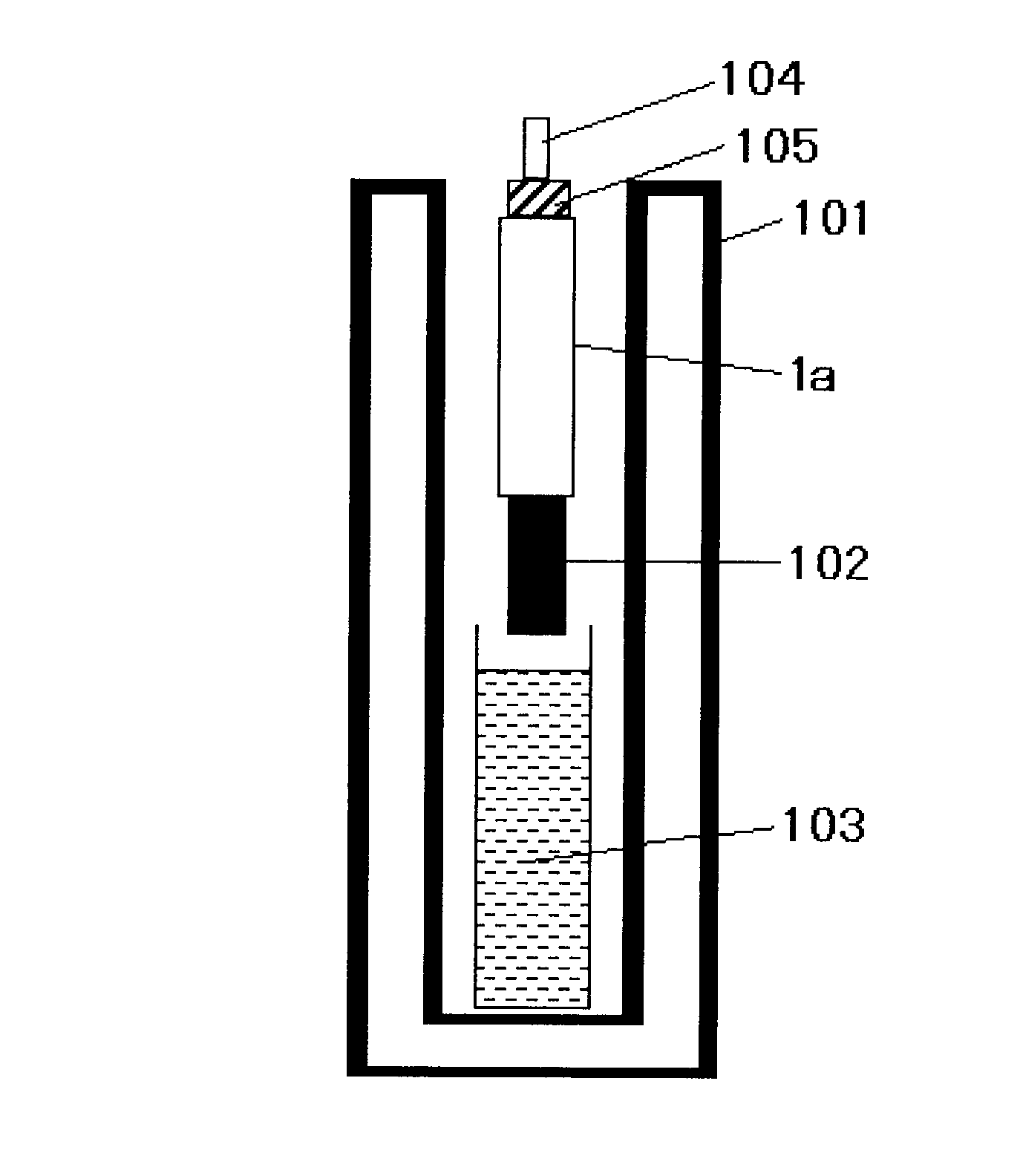
[0092]The electrophotographic photoconductor of the present invention can be obtained by applying the magnetic field to the electrophotographic photoconductor either during or after the formation of the photosensitive layer containing the charge transporting material having a triarylamine structure.
[0093]A coating liquid for the photosensitive layer is started to be coated, and then either during or after the formation of the photosensitive layer containing the charge transporting material having a triarylamine structure, the magnetic field can be applied at any time, and is preferably applied to the electrophotographic photoconductor either while the coating liquid for the photosensitive layer is coated or immediately after the coating liquid for the photosensitive layer is coated and before cured. This is because, the charge transporting material having a triarylamine structure easily moves before the photosensitive layer is cured. In the present invention, “cured” means that the layer does not stick to a finger when it is touched with the finger.

Problems solved by technology

In the laminated organic photoconductor, the reduction of resolution, photosensitivity, and charge mobility, and rise of residual potential are recognized as big problems for improving image quality and speeding-up the image forming apparatus.
Additionally, the reduction of photosensitivity and the charge mobility and rise of the residual potential may be caused by that the charge are trapped in a process of moving by hopping in the charge transporting material.
However, the charge transporting materials used for these conventional arts do not satisfy electrophotographic property, and have not been practically applied.
However, these techniques may be effective for improving the wear resistance and smoothing property of the undercoat layer, but not actually effective for essential properties for improving image quality of the image forming apparatus, such as resolution, sensitivity, residual potential, and mobility, these are rather sacrificed.

Method used


Image

  • Electrophotographic photoconductor and method for producing the same, image forming apparatus, and process cartridge
  • Electrophotographic photoconductor and method for producing the same, image forming apparatus, and process cartridge
  • Electrophotographic photoconductor and method for producing the same, image forming apparatus, and process cartridge

Examples


example 1

Stilbene

[0258]First, a coating liquid for an undercoat layer and a coating liquid for a charge generating layer of the following compositions were coated by immersion coating and dried one by one in an oven to form an undercoat layer of 3.5 μm-thick and a charge generating layer of 0.2 μm-thick on an aluminum cylinder having a circular cross section with a diameter of 30 mm. Specifically, the drying condition of each layer was as follows: the undercoat layer was dried at 130° C. for 20 minutes; and the charge generating layer was dried at 90° C. for 20 minutes.

[0259]

The composition of the coating liquid for the undercoat layerTitanium oxide (CR-EL, by Ishihara Sangyo Ltd.)50partsAlkyd resin Bekolite M6401-50, Solid Content: 50% by14partsmass, by Dainippon Ink and Chemicals, Inc.Melamine resin L-145-60, Solid Content: 60% by mass, by8partsDainippon Ink and Chemicals, Inc.2-butanone120partsThe composition of the coating liquid for the charge generating layerTitanyl phthalocyanine show...

example 2

[0265]A photoconductor 2 was produced in the same manner as Example 1, except that the charge transporting material in Example 1 was changed to the charge transporting material represented by the following Structural Formula:

[0266]

example 3

[0267]A photoconductor 3 was produced in the same manner as Example 1, except that the charge transporting material in Example 1 was changed to the charge transporting material represented by the following Structural Formula:

[0268]


PUM


Abstract

There is provided an electrophotographic photoconductor containing a conductive substrate, and a photosensitive layer, disposed thereon, containing a charge transporting material having a triarylamine structure represented by General Formula 1, and wherein the photosensitive layer satisfies Mathematical Formula 1 when peak heights in raman scattering spectra of the triarylamine structure are measured at a wavenumber of 1,324±2 cm−1 by a confocal raman spectroscopy using z-polarized light:where Ar1, Ar2, and Ar3 are substituted or unsubstituted aromatic hydrocarbon groups, and Ar1 and Ar2, Ar2 and Ar3, and Ar3 and Ar1 are optionally combined to form heterocyclic rings, respectively,ε=I(inside) / I(surface)≧1.1  Mathematical Formula 1where I(inside) represents the peak height in of the raman scattering spectrum obtained at a depth of 5 μm or more from the photosensitive layer surface and I(surface) represents the peak height in the raman scattering spectrum obtained at a depth of less than 5 μm from the photosensitive layer surface.

Description

BACKGROUND OF THE INVENTION[0001]1. Field of the Invention[0002]The present invention relates to an electrophotographic photoconductor having a high resolution and photosensitivity, low residual potential and excellent electrostatic property and a method for producing the electrophotographic photoconductor, and an image forming apparatus and a process cartridge used for the image forming apparatus by using the electrophotographic photoconductor.[0003]2. Description of the Related Art[0004]In recent years, image forming apparatuses such as laser printers and digital copiers using an electrophotographic system, provide an image with improved image quality and stability and are broadly used. Recently, speeded-up, downsized, and full-colored image forming apparatuses are rapidly developed, and an electrophotographic photoconductor (hereinafter, referred to as a photoconductor) used for the image forming apparatuses, is needed to improve further carrier mobility and photosensitivity, and...

Claims


Application Information

Patent Timeline
Patent Type & Authority Patents(United States)
IPC IPC(8): G03G5/05
CPCG03G5/047G03G5/0607G03G5/0614G03G5/0674G03G5/0629G03G5/0668G03G5/0672G03G5/0622G03G5/061443G03G5/06147G03G5/061473
Inventor TADA, HIROMITAMOTO, NOZOMUOHTA, KATSUICHI
Owner RICOH KK
Learn More