IGBT semiconductor device

a semiconductor device and semiconductor technology, applied in semiconductor devices, semiconductor/solid-state device details, electrical devices, etc., can solve the problems of reducing the efficiency of injecting carriers from the collector layer into the drift layer, and the method of patent document 1 cannot be adopted in the igbt, so as to increase the dielectric breakdown strength and increase the on-resistance

Active Publication Date: 2011-07-05
DENSO CORP
View PDF25 Cites 12 Cited by
  • Summary
  • Abstract
  • Description
  • Claims
  • Application Information

AI Technical Summary

Benefits of technology

[0010]However, the method of Patent Document 1 cannot be adopted in the IGBT. In the case of the IGBT, the buffer layer is formed at the back surface of the semiconductor layer (drift layer), thereby to prevent the depletion layer from extending to the collector layer. The buffer layer includes impurities of the same conductivity type as that of the drift layer, at a higher concentration than the drift layer. If the technique of Patent Document 1, in which the thickness of the buffer layer in the active region is increased and its thickness in the peripheral region is decreased, is applied, the on-voltage of the IGBT may increase. If the thickness of the buffer layer is increased, the efficiency of injecting carriers from the collector layer into the drift layer may decrease. If the thickness of the buffer layer is increased in the active region, the efficiency of injecting carriers may decrease and the on-voltage may increase. One problem to be solved by the present invention is to provide an IGBT in which the dielectric breakdown strength is improved without increasing the on-voltage.
[0011]One technique taught in the present specification makes the thickness of the drift layer in the peripheral region to be greater than that of the drift layer in the active region. Further, the amount of carriers injected into the drift layer is suppressed more in the peripheral region than in the active region. These two operations improve the dielectric breakdown strength of the peripheral region.

Problems solved by technology

However, the method of Patent Document 1 cannot be adopted in the IGBT.
If the thickness of the buffer layer is increased, the efficiency of injecting carriers from the collector layer into the drift layer may decrease.

Method used


Image

  • IGBT semiconductor device
  • IGBT semiconductor device
  • IGBT semiconductor device

Examples


first embodiment

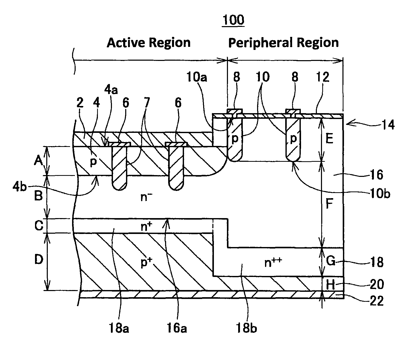
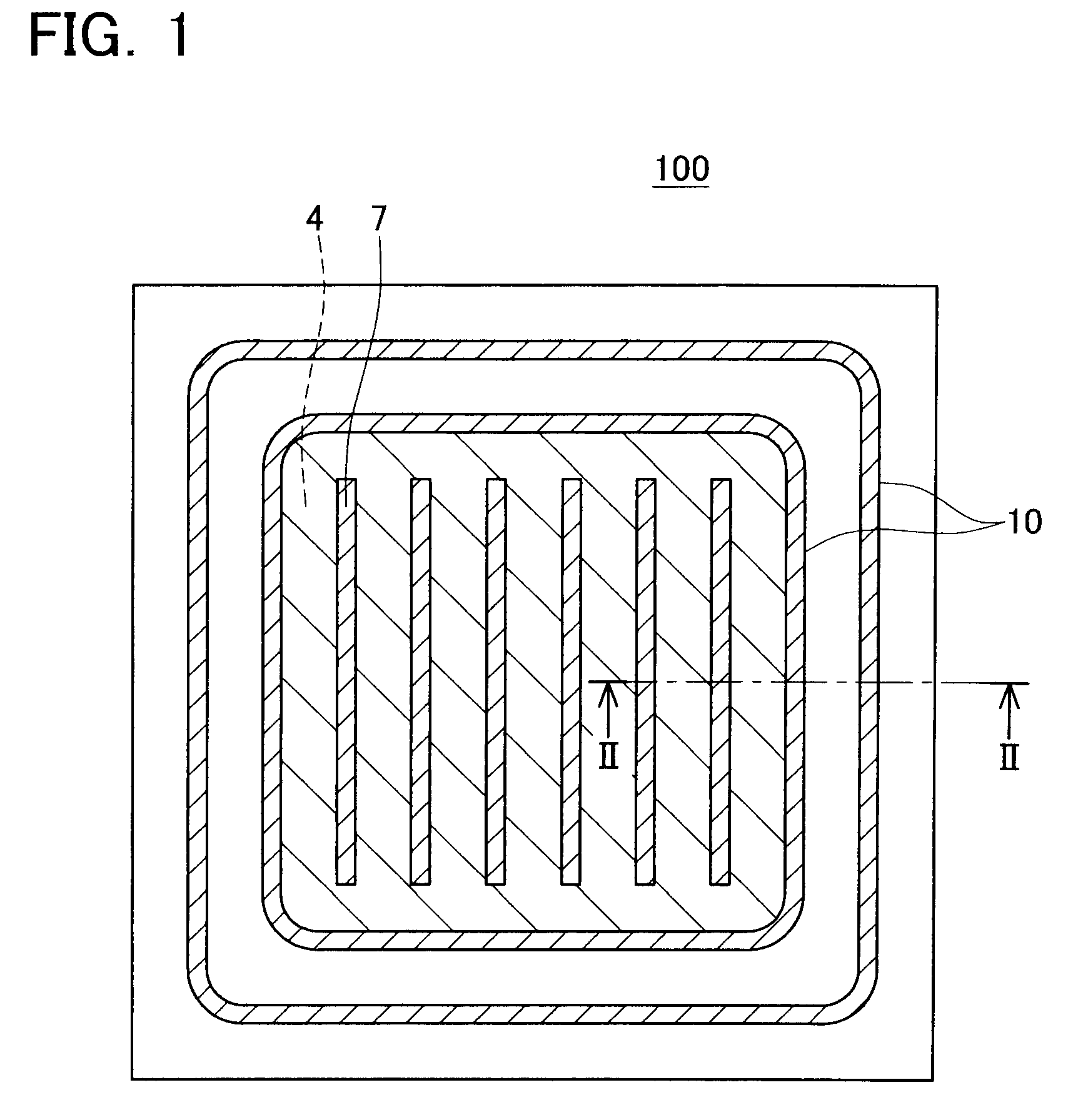
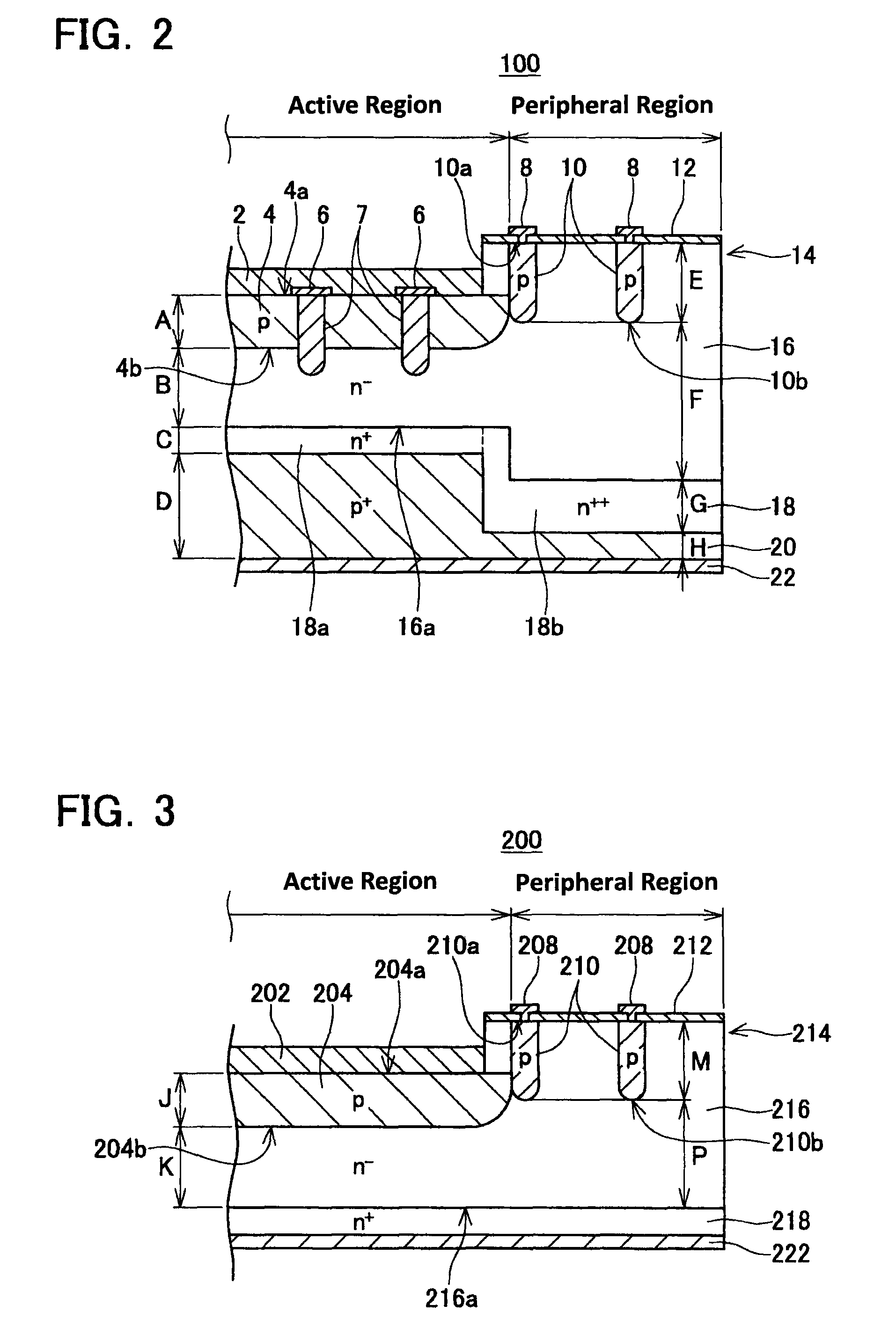
[0029]A semiconductor device of the first embodiment will be explained with reference to FIGS. 1, 2. The semiconductor device of the present embodiment is an example in which the present invention has been applied to an IGBT. FIG. 1 is a schematic plan view of an IGBT 100. FIG. 2 is a schematic cross-sectional view of the IGBT 100 viewed along the line II-II of FIG. 1.

[0030]First, an outline of the configuration of the IGBT 100 will be given. The IGBT 100 is formed on a semiconductor substrate 14. Below, the “semiconductor substrate 14” is termed simply “substrate 14”. A metal collector electrode 22 is formed on a back surface of the substrate 14. A p+-type collector layer 20 (third semiconductor layer) is formed on an upper surface of the collector electrode 22, i.e. on a bottom layer of the substrate 14. An n-type buffer layer 18 (high impurity concentration layer) is formed on the collector layer 20. The concentration of the n-type impurities in the buffer layer 18 will be descri...

second embodiment

[0050]Next, a semiconductor device of the second embodiment will be explained with reference to FIG. 3. The semiconductor device of the present embodiment is a diode. FIG. 3 is a schematic cross-sectional view of a diode 200 of the second embodiment.

[0051]The diode 200 is formed on a semiconductor substrate 214 (termed substrate 214 below). A metal cathode electrode 222 is formed on a back surface of the substrate 214. An n+-type cathode region 218 (high impurity concentration layer) is formed on the cathode electrode 222. I.e., the high impurity concentration layer 218 is formed on a bottom layer of the substrate 214. An n-type semiconductor layer 216 is formed on the high impurity concentration layer 218.

[0052]A p-type anode region 204 (first semiconductor region) is formed within a range of a part of a surface layer of the semiconductor layer 216 (in FIG. 3, an upper surface side of the semiconductor layer 216). A p-type guard ring 210 (second semiconductor region) that surrounds...


PUM


Abstract

To provide a semiconductor device in which dielectric breakdown strength in a peripheral region is increased without increasing on-resistance. An IGBT comprises a body region, guard ring, and collector layer. The body region is formed within an active region in a surface layer of a drift layer. The guard ring is formed within a peripheral region in the surface layer of the drift layer, and surrounds the body region. The collector layer is formed at a back surface side of the drift layer, and is formed across the active region and the peripheral region. A distance F between a back surface of the guard ring and the back surface of the drift layer is greater than a distance between a back surface of the body region and the back surface of the drift layer. A thickness H of the collector layer in the peripheral region is smaller than a thickness D of the collector layer in the active region.

Description

[0001]This application is a national phase application of International Application No. PCT / JP2008 / 070109, filed Nov. 5, 2008, and claims priority to Japanese Patent Application No. 2007-289536, filed on Nov. 7, 2007, the contents of both of which are hereby incorporated by reference into the present application. The present invention relates to a semiconductor device whose dielectric breakdown strength (voltage resistance) is increased without increasing its resistance while conducting. For example, the present invention relates to an IGBT with low on-voltage and high dielectric breakdown strength, or a diode with low forward voltage drop and high dielectric breakdown strength. In the present specification, “low resistance while conducting” means that forward voltage drop, on-resistance, or on-voltage is low.TECHNICAL FIELDBackground Art[0002]A semiconductor device is known that comprises a semiconductor substrate which, in a plan view, includes an active region in which a semicond...

Claims


Application Information

Patent Timeline
Patent Type & Authority Patents(United States)
IPC IPC(8): H01L29/76H01L29/74H01L29/94
CPCH01L29/0657H01L29/0696H01L29/404H01L29/7397H01L29/8611H01L29/0619H01L2924/10155
Inventor HARA, MASAFUMI
Owner DENSO CORP
Why Eureka
Try Eureka