Sidewall coating for non-uniform spin momentum-transfer magnetic tunnel junction current flow

a momentum-transfer magnetic tunnel junction and current flow technology, which is applied in the direction of magnetic field-controlled resistors, digital storage, instruments, etc., can solve the problems of low current flow rate, soft errors, and undesirable high current levels, and achieve the effect of enhancing current flow and enhancing current flow

Active Publication Date: 2011-08-02
INT BUSINESS MASCH CORP
View PDF8 Cites 31 Cited by
  • Summary
  • Abstract
  • Description
  • Claims
  • Application Information

AI Technical Summary

Benefits of technology

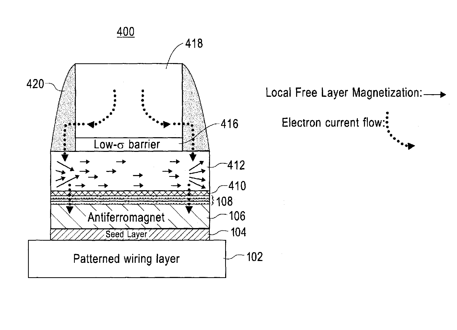
[0003]In view of the problems discussed above, it would be valuable to create a structure where one increases the relative amount of current flow along the edges of a device with in-plane magnetization, as the edges of the device will exhibit magnetization with a substantial out-of-plane component, due to magnetic edge effects. The higher current in edge regions where out-of-plane magnetization is present would make for more efficient transfer of spin torque from the electrons to the MTJ free layer, as the spin torque coupling is substantial only for the out-of-plane component of magnetization of the MTJ free layer.
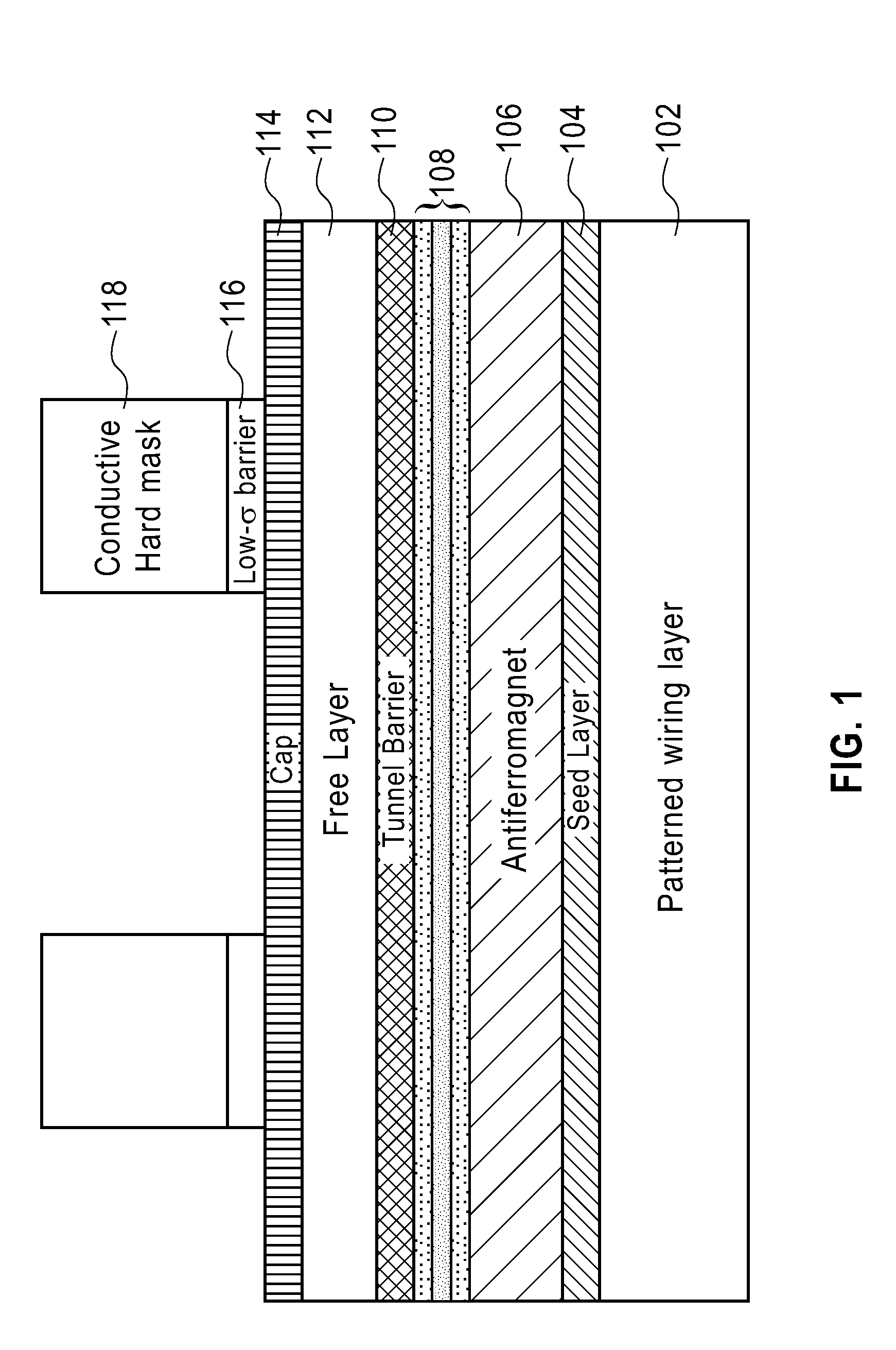
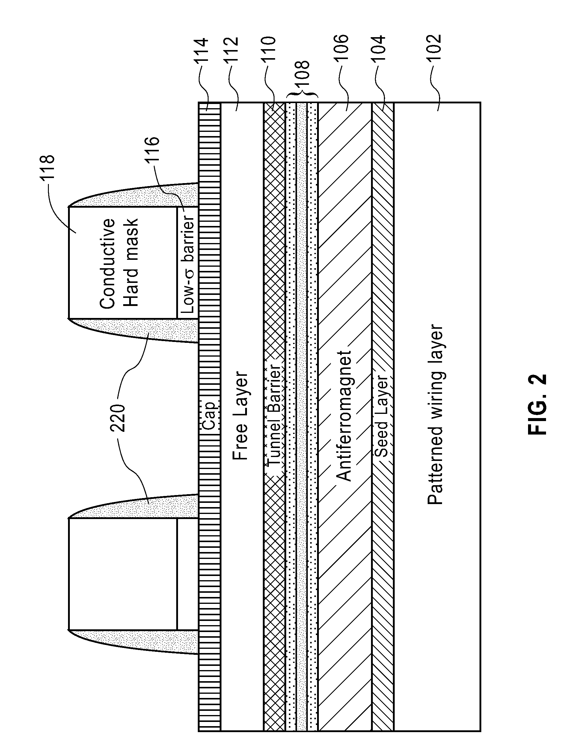
[0005]In another embodiment a magnetic tunnel junction device is disclosed. The magnetic tunnel junction device comprises a substrate including a patterned wiring layer. A magnetic tunnel junction stack is formed over the wiring layer. A low-conductivity layer is formed over the magnetic tunnel junction stack. A conductive hard mask is formed over the low-conductivity layer. The hard mask and low-conductivity layer are etched down to the free layer. A spacer material is deposited over the etched structure. The spacer material comprises a different electrical conductivity than the low conductivity layer. The spacer material is etched from horizontal surfaces so that the spacer material remains only on sidewalls of the hard mask and the stud. The device is further defined by etching the stack materials which are not protected by the hard mask or the sidewall-spacer material. This etch is tuned to leave behind the sidewall-spacer material as a conductive link between the free layer and the conductive hard mask, around the low-conductivity layer. A difference in electrical conductivity between the stud and the spacer material enhances current flow along the edges of the free layer within the magnetic tunnel junction stack and through the spacer material formed on the sidewalls.
[0006]In yet another embodiment, an integrated circuit is disclosed. The integrated circuit comprises a circuit supporting substrate having an electrical circuit disposed thereon and a magnetic tunnel junction device. The magnetic tunnel junction device comprises a substrate including a patterned wiring layer. A magnetic tunnel junction stack is formed over the wiring layer. A low-conductivity layer is formed over the magnetic tunnel junction stack. A conductive hard mask is formed over the low-conductivity layer. The hard mask and low-conductivity layer are etched down to the free layer. A spacer material is deposited over the etched structure. The spacer material comprises a different electrical conductivity than the low conductivity layer. The spacer material is etched from horizontal surfaces so that the spacer material remains only on sidewalls of the hard mask and the stud. The device is further defined by etching the stack materials which are not protected by the hard mask or the sidewall-spacer material. This etch is tuned to leave behind the sidewall-spacer material as a conductive link between the free layer and the conductive hard mask, around the low-conductivity layer. A difference in electrical conductivity between the stud and the spacer material enhances current flow along the edges of the free layer within the magnetic tunnel junction stack and through the spacer material formed on the sidewalls.

Problems solved by technology

These high current levels are undesirable since they require large switching transistors, and consequently large cell sizes.
This is a poorly controlled approach, and leads to soft errors, slow write times, and the need for high switching currents.

Method used


Image

  • Sidewall coating for non-uniform spin momentum-transfer magnetic tunnel junction current flow
  • Sidewall coating for non-uniform spin momentum-transfer magnetic tunnel junction current flow
  • Sidewall coating for non-uniform spin momentum-transfer magnetic tunnel junction current flow

Examples


Embodiment Construction

[0011]As required, detailed embodiments of the present invention are disclosed herein; however, it is to be understood that the disclosed embodiments are merely examples of the invention, which can be embodied in various forms. Therefore, specific structural and functional details disclosed herein are not to be interpreted as limiting, but merely as a basis for the claims and as a representative basis for teaching one skilled in the art to variously employ the present invention in virtually any appropriately detailed structure and function. Further, the terms and phrases used herein are not intended to be limiting; but rather, to provide an understandable description of the invention.

[0012]The terms “a” or “an”, as used herein, are defined as one or more than one. The term plurality, as used herein, is defined as two or more than two. The term another, as used herein, is defined as at least a second or more. The terms including and / or having, as used herein, are defined as comprisin...


PUM


Abstract

A magnetic tunnel junction device comprises a substrate including a patterned wiring layer. A magnetic tunnel junction (MTJ) stack is formed over the wiring layer. A low-conductivity layer is formed over the MTJ stack and a conductive hard mask is formed thereon. A spacer material is then deposited that includes a different electrical conductivity than the low conductivity layer. The spacer material is etched from horizontal surfaces so that the spacer material remains only on sidewalls of the hard mask and a stud. A further etch process leaves behind the sidewall-spacer material as a conductive link between a free magnetic layer and the conductive hard mask, around the low-conductivity layer. A difference in electrical conductivity between the stud and the spacer material enhances current flow along the edges of the free layer within the MTJ stack and through the spacer material formed on the sidewalls.

Description

[0001]The present invention generally relates to the field of semiconductors, and more particularly relates to magneto-resistive random access memory (MRAM) comprising a sidewall coating for non-uniform Spin Momentum Transfer (SMT) magnetic tunnel junction (MTJ) current flow, and a method for fabricating the same.BACKGROUND OF THE INVENTION[0002]State-of-the-art methods for storing data in SMT MRAM generally require high current levels to switch the free layer between high and low resistance states. These high current levels are undesirable since they require large switching transistors, and consequently large cell sizes. In-plane magnetization materials and devices are presently far simpler to create than out-of-plane magnetization structures, but the spin torque coupling from electron spins to the MTJ free layer is nearly absent when the magnetic moment of the MTJ free layer is in-plane (parallel to tunnel barrier). This is because the electrons traverse the tunnel barrier in a di...

Claims


Application Information

Patent Timeline
Patent Type & Authority Patents(United States)
IPC IPC(8): H01L21/00H01L21/02
CPCG11C11/16H01L43/12H01L43/08H01L29/66984H01L29/82G11C11/161H10N50/01H10N50/10
Inventor GAIDIS, MICHAEL C.
Owner INT BUSINESS MASCH CORP
Why Eureka
Try Eureka