

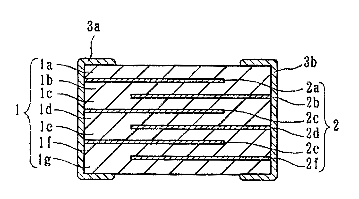
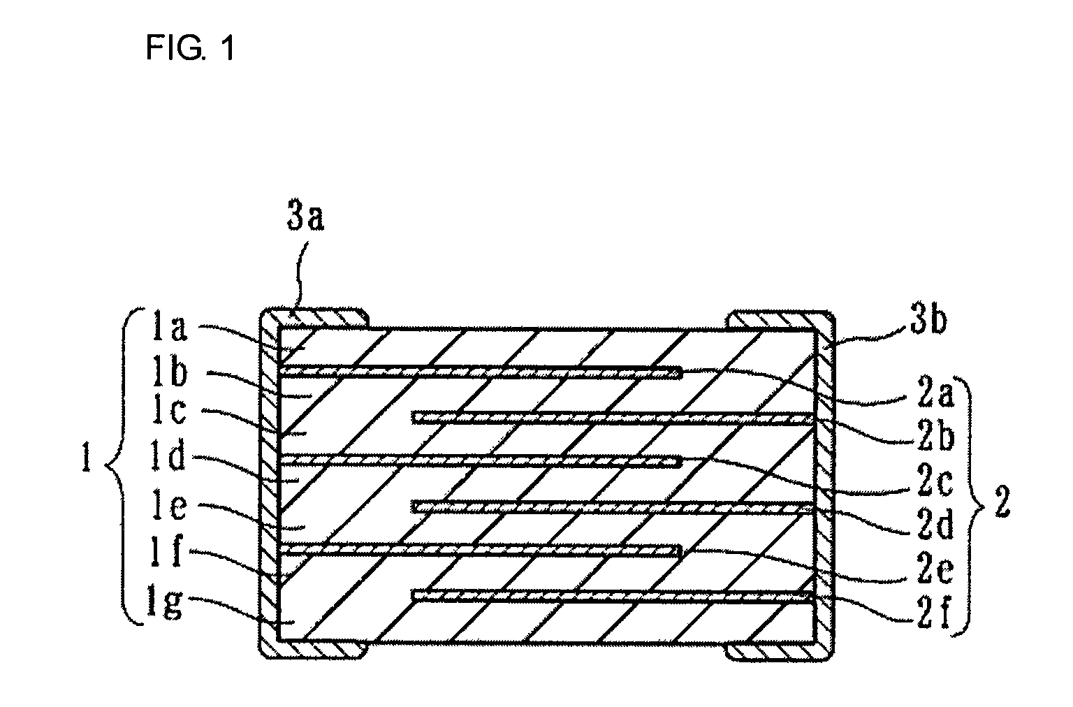
Semiconductor ceramic and multilayered-type semiconductor ceramic capacitor
a semiconductor ceramic and semiconductor technology, applied in the direction of fixed capacitors, basic electric elements, electrical appliances, etc., can solve the problems of short-circuit failure, reduced relative dielectric constant, temperature characteristics of capacitance, etc., and achieves lower cost, higher capacitance, and small layer thickness
- Summary
- Abstract
- Description
- Claims
- Application Information
AI Technical Summary
Benefits of technology
Problems solved by technology
Method used
Image

Examples
example 1
[0081]As ceramic starting materials, SrCO3, LaCl3, and TiO2 having a specific surface area of 30 m2 / g (average grain size: about 30 nm) were prepared, and these ceramic starting materials were weighed so as to satisfy the compositions shown in Table 1. Furthermore, an ammonium salt of polycarboxylic acid in an amount of 2 parts by weight relative to 100 parts by weight of the weighed materials was added as a dispersant, and the resulting mixture was placed in a ball mill together with PSZ balls with a diameter of 2 mm and water. Wet mixing was performed in the ball mill for 16 hours to form a slurry.
[0082]Next, the slurry was dried by evaporation, and then a calcination treatment was carried out in an air atmosphere at 1,400° C. for two hours. Thereby, a calcined powder of a semiconductor in which the La element had been dissolved to form a solid solution was obtained.
[0083]Ethyl silicate (Si(OC2H5)4) was then added so that the molar quantity of SiO2 contained relative to 100 moles ...
example 2
[0101]As ceramic starting materials, Sr(OH)2.8H2O, LaCl3, and TiO2 having a specific surface area of 300 m2 / g (average grain size: about 5 nm) were prepared, and these ceramic starting materials were weighed so as to satisfy the compositions shown in Table 2. Next, pure water was added thereto such that the volume of the solid solution slurry was 4.0×10⁻⁴ m3 (400 cc), and the resulting mixture was placed in a beaker made of a fluorocarbon resin. Then, the beaker was set in a stirring-type autoclave, and a hydrothermal synthesis reaction was caused at a temperature of 200° C. and at 8.5 s−1 (500 rpm) (pressure: about 1.5×10⁵ Pa) for four hours. Thereby, a slurry in which the La element was homogeneously contained at the nanometer level was formed.
[0102]The resulting slurry was dried by evaporation to form a powder. Then, an ammonium salt of polycarboxylic acid in an amount of 2 parts by weight relative to 100 parts by weight of the powder was added as a dispersant, and the resulting ...
example 3
[0108]Sample Nos. 31 to 33 were formed by the same method / procedure as in Example 1 except that SmCl3 was used as the additive material instead of LaCl3. The average crystal grain size, the apparent relative dielectric constant ∈rAPP, and the dielectric loss tan δ, were measured by the same methods / procedures as in Example 1.
[0109]Table 3 shows the compositions and measurement results for Sample Nos. 31 to 33.
[0110]
TABLE 3ElementDielectric characteristicsdissolved toApparentMixingform solidrelativeDielectricAveragemolarsolutionAdditive materialdielectriclosscrystalSampleratioSmMnOSiO2constanttan δgrain sizeNo.m(mol)(mol)(mol)εrAPP(%)(μm)311.0021.20.40.0558501.40.6321.0041.60.5063100.90.8331.0081.80.90.0767500.80.7
[0111]In Example 3, Sm was used as the element dissolved to form a solid solution. In the resulting semiconductor ceramics, the average crystal grain size was 0.6 to 0.8 μm (i.e., 1.0 μm or less), and moreover, the apparent relative dielectric constant ∈rAPP was 5,850 to 6,...
PUM
| Property | Measurement | Unit |
|---|---|---|
| grain size | aaaaa | aaaaa |
| grain size | aaaaa | aaaaa |
| thickness | aaaaa | aaaaa |
Abstract
Description
Claims
Application Information