OLED device with embedded chip driving

a technology of embedded chips and oled devices, which is applied in the direction of discharge tubes/lamp details, discharge tubes luminescent screens, electric discharge lamps, etc., can solve the problems of low oled display quality, and unstable amorphous silicon, etc., and achieve the effect of reducing the thickness of the display

Active Publication Date: 2011-08-16
X DISPLAY CO TECH LTD +1
View PDF11 Cites 317 Cited by
  • Summary
  • Abstract
  • Description
  • Claims
  • Application Information

AI Technical Summary

Benefits of technology

[0009]It is an object of present invention to provide an improved method of producing an electroluminescent OLED display having chiplets driving elements where the chiplets are reduced in size and therefore cost. It is a further object of the present invention to reduce the thickness of the display having chiplets driving elements. It is a further object of this invention to provide ultra-thin chiplet driving elements which are interconnected to the OLED pixel elements using thin film metal deposition processes. This object is achieved by an electroluminescent device having a plurality of current driven pixels arranged in rows and columns disposed over a substrate, such that when current is provided to a pixel it produces light, comprising:

Problems solved by technology

The properties of such thin film semiconductors are, however, often not sufficient for constructing a high quality OLED display.
Amorphous silicon, for example, is unstable in that its threshold voltage (Vth) and carrier mobility shifts over extended periods of use.
Since OLED devices operate by current injection, variability in the TFTs can result in variability of the luminance of the OLED pixels and degrade the visual quality of the display.
Novel compensation schemes, such as adding additional TFT circuitry in each pixel, have been proposed to compensate for TFT variability, however, such compensation adds complexity which can negatively impact yield, cost, or reduce the OLED emission area.
Furthermore, as thin film transistor fabrication processes are applied to larger substrates such as used for large flat-panel television applications, the variability and process cost increase.
Thinning the substrate in this fashion is difficult and at low thicknesses, the crystalline substrate is very fragile and easily broken.
The thick chiplets of Matsumura result in substantial topography across the substrate, which makes the subsequent deposition and patterning of metal layers over the chiplets difficult.
For example, Matsumura describes concave deformations as one undesirable effect.
Another disadvantage of the process taught by Matsumura is that the surface area of the chiplets must be large enough to be picked up by the vacuum hole fixture.
First, it is difficult to achieve high quality semiconductors since thin film layers of semiconductor must be formed over a release layer.
Second, this approach requires the additional cost of forming in isolated beads of conductive adhesive.
Third, it is difficult to achieve a high yield of good quality electrical connections by aligning to the small beads of conductive adhesive.

Method used


Image

  • OLED device with embedded chip driving
  • OLED device with embedded chip driving
  • OLED device with embedded chip driving

Examples


Embodiment Construction

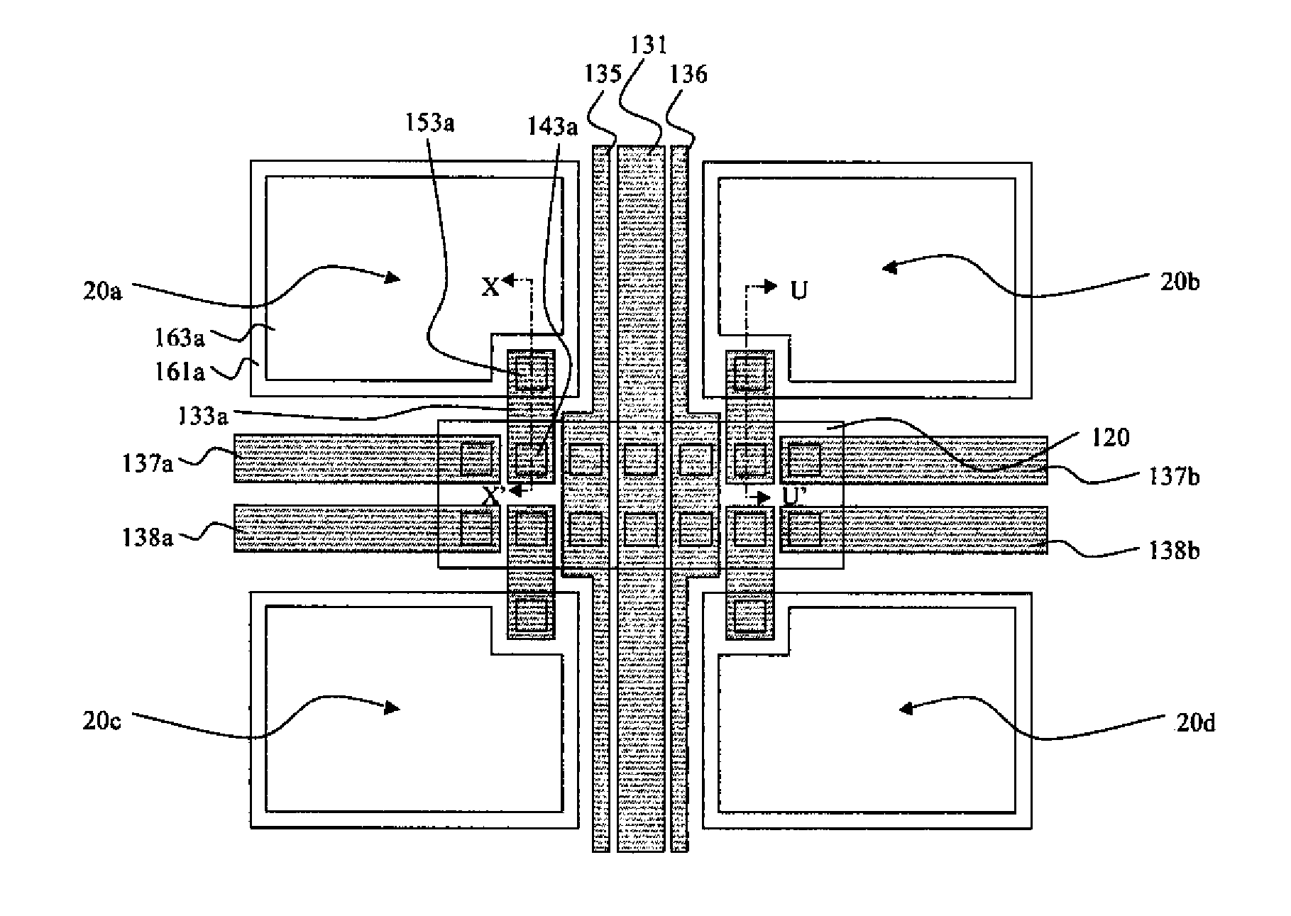
[0028]FIG. 1 shows a layout view of a group of four pixels (20a, 20b, 20c and 20d) elements of an OLED display device according to the present invention. Each of the four pixels can be arranged to emit a different color, such as red, green, blue and white (RGBW). FIG. 1 represents a portion of a full display where the full display would be constructed of an array of such groups of pixels arranged in many rows and columns. For example, a modern television would be constructed having 1920 rows and 1080 columns of such groups of pixels.

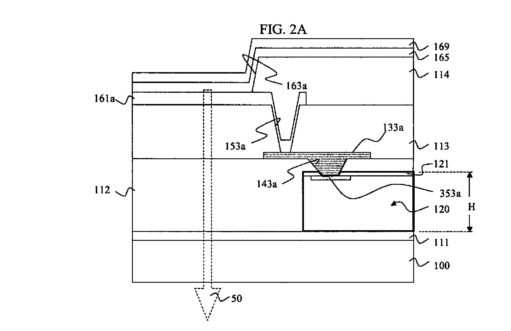
[0029]A chiplet 120 is arranged to control the electrical current to pixels 20a, 20b, 20c and 20d. A chiplet is a separately fabricated integrated circuit which is mounted and embedded into the display device. Much like a conventional microchip (or chip) a chiplet is fabricated from a substrate and contains integrated transistors as well as insulator layers and conductor layers which are deposited and then patterned using photolithographic methods in a s...


PUM


Abstract

An electroluminescent device having a plurality of current driven pixels arranged in rows and columns, such that when current is provided to a pixel it produces light, including each pixel having first and second electrodes and current responsive electroluminescent media disposed between the first and second electrodes; at least one chiplet having a thickness less than 20 micrometers; including transistor drive circuitry for controlling the operation of at least four pixels, the chiplet being mounted on a substrate and having connection pads; a planarization layer disposed over at least a portion of the chiplet; a first conductive layer over the planarization layer and connected to at least one of the connection pads; and a structure for providing electrical signals through the first conductive layer and at least one of the connection pads of the chiplet so that the transistor drive circuitry of the chiplet controls current to the four pixels.

Description

FIELD OF THE INVENTION[0001]The present invention relates to an electroluminescent display with semiconductor driving elements.BACKGROUND OF THE INVENTION[0002]In the simplest form, an organic electroluminescent (EL) device is comprised of an organic electroluminescent media disposed between first and second electrodes serving as an anode for hole injection and a cathode for electron injection. The organic electroluminescent media supports recombination of holes and electrons that yields emission of light. These devices are also commonly referred to as organic light-emitting diodes, or OLEDs. A basic organic EL element is described in U.S. Pat. No. 4,356,429. In order to construct a pixelated OLED display device that is useful as a display such as, for example, a television, computer monitor, cell phone display, or digital camera display, individual organic EL elements can be arranged as pixels in a matrix pattern. These pixels can all be made to emit the same color, thereby produci...

Claims


Application Information

Patent Timeline
Patent Type & Authority Patents(United States)
IPC IPC(8): H05B33/08H01L51/00H05B44/00
CPCH01L27/3248H01L27/3255H01L27/322H01L27/3276H01L2227/323H10K59/38H10K59/129H10K59/123H10K59/131H10K59/1201H10K10/46
Inventor WINTERS, DUSTIN L.HAMER, JOHN W.PARRETT, GARYBOWER, CHRISTOPHERMENARD, ETIENNE
Owner X DISPLAY CO TECH LTD
Why Eureka
Try Eureka