
Thin film transistor, method of manufacturing the same, and electronic device using the same

a technology of thin film transistors and manufacturing methods, applied in non-linear optics, instruments, nanoinformatics, etc., can solve the problems of high cost of vacuum film forming apparatuses used in cvd and sputtering methods and photolithography apparatuses, and the inability to use films with low heat resistance, such as plastic substrates, to achieve the effect of low cost and easy process

Active Publication Date: 2011-09-06
SAMSUNG DISPLAY CO LTD
View PDF7 Cites 55 Cited by
  • Summary
  • Abstract
  • Description
  • Claims
  • Application Information

AI Technical Summary

Benefits of technology

The present invention provides a thin film transistor that is easy to manufacture and has high performance. The transistor includes a semiconductor layer made of a complex oxide containing zinc and at least one selected from a group consisting of indium, gallium, and rhodium. The method of manufacturing the transistor includes forming a layer of semiconductor fine particles composed of the complex oxide and subjecting it to a heat treatment at a temperature of 150°C or higher. The invention also provides an electronic device including the thin film transistor. The technical effects of the invention are that it allows for the manufacture of a high-performance thin film transistor at low cost and on a substrate made of resin.

Problems solved by technology

Vacuum film-forming apparatuses used for the CVD and sputtering methods and photolithography apparatuses are both expensive, and thus the cost of these apparatuses accounts for a significant part of the manufacturing cost of liquid crystal panels.
In addition, amorphous silicon films and polysilicon films are fabricated at high temperatures, and therefore substrates having low heat resistance, such as a plastic substrate, cannot be used for such films.
However, these semiconductor nanomaterials are strongly anisotropic in their properties.
However, it is not easy, in the state of the art, to orient the nanomaterials.
However, these semiconductor films have lower mobilities than that of an amorphous silicon film, which is not satisfactory in their performance to drive liquid crystal elements and organic EL elements.
However, these TFTs have not yet achieved successfully both the ease of the manufacturing process and the satisfactory performance, and thus have not yet been put to practical use.

Method used


Image

  • Thin film transistor, method of manufacturing the same, and electronic device using the same
  • Thin film transistor, method of manufacturing the same, and electronic device using the same
  • Thin film transistor, method of manufacturing the same, and electronic device using the same

Examples


first embodiment

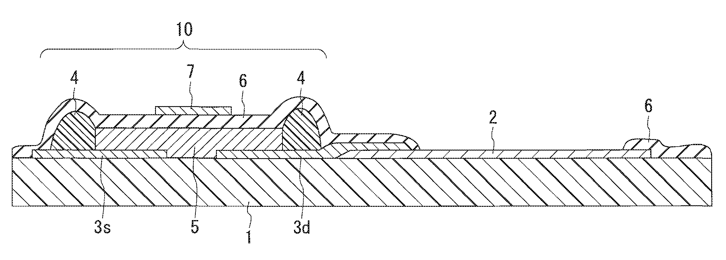
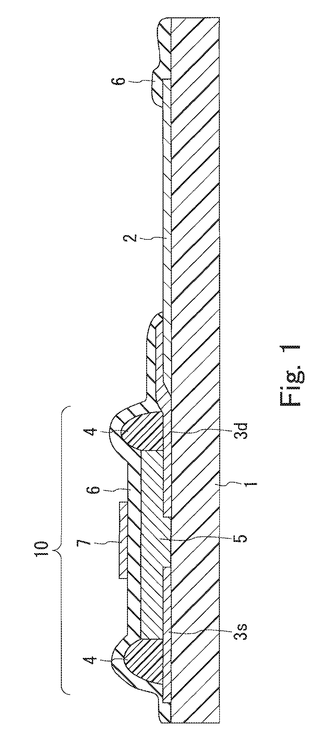
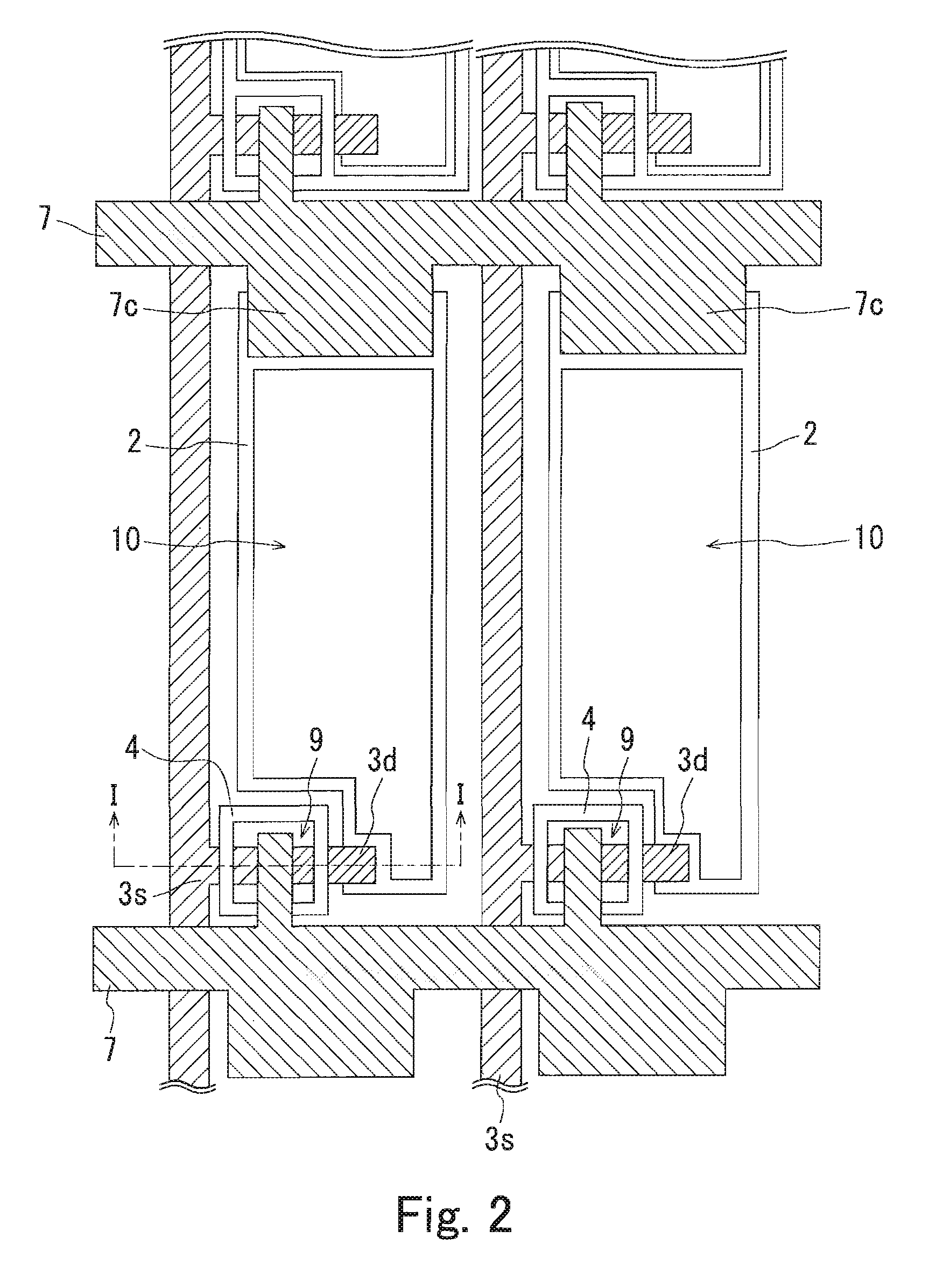
[0036]In the first embodiment, an example of the TFT of the present invention that is formed on a substrate of a liquid crystal panel is described. FIG. 1 shows a cross-sectional view of a TFT 10 according to the first embodiment, and FIG. 2 shows a plan view thereof. FIG. 1 is a cross section of the TFT 10 viewed along the line I-I of FIG. 2. For ease of understanding, FIG. 2 does not show the semiconductor layer 5 and the insulating layer 6. In FIG. 2, the gate electrode, the source electrode and the drain electrode are hatched.

[0037]The TFT 10 is formed on a substrate 1. The TFT 10 includes a source electrode 3s, a drain electrode 3d, a semiconductor layer 5, an insulating layer 6, and a gate electrode 7.

[0038]The source electrode 3s and the drain electrode 3d are disposed on the substrate 1 at a distance from each other. The semiconductor layer 5 is formed on the substrate 1, the source electrode 3s and the drain electrode 3d. The semiconductor layer 5 is formed inside a bank 4....


PUM


Abstract

A thin film transistor according to the present invention includes: a semiconductor layer (5); a source electrode (3s) and a drain electrode (3d) that each are connected to the semiconductor layer (5); an insulating layer (6) that is formed adjacent to the semiconductor layer (5); and a gate electrode (7) that faces the semiconductor layer (5) across the insulating layer (6). The semiconductor layer (5) includes an aggregate of semiconductor fine particles composed of a complex oxide. The complex oxide contains zinc and at least one selected from a group consisting of indium, gallium and rhodium.

Description

TECHNICAL FIELD[0001]The present invention relates to a thin film transistor, a method of manufacturing the same, and an electronic device using the same.BACKGROUND ART[0002]Thin film transistors (TFTs) using amorphous silicon or polysilicon have been put to practical use as drive elements for liquid crystal displays. Generally, these TFTs are formed in a manufacturing process in which various methods such as CVD, sputtering and photolithography are used in combination. Vacuum film-forming apparatuses used for the CVD and sputtering methods and photolithography apparatuses are both expensive, and thus the cost of these apparatuses accounts for a significant part of the manufacturing cost of liquid crystal panels. In addition, amorphous silicon films and polysilicon films are fabricated at high temperatures, and therefore substrates having low heat resistance, such as a plastic substrate, cannot be used for such films.[0003]As a method of forming a TFT on a plastic substrate, for exa...

Claims


Application Information

Patent Timeline
Patent Type & Authority Patents(United States)
IPC IPC(8): H01L29/26H01L29/786
CPCB82Y10/00H01L29/0665H01L29/0669H01L29/0673H01L29/41733H01L29/7869G02F1/1368G02F2202/36
Inventor WAKITA, NAOHIDE
Owner SAMSUNG DISPLAY CO LTD
Learn More