Electrical contacts on top of waveguide structures for efficient optical modulation in silicon photonic devices

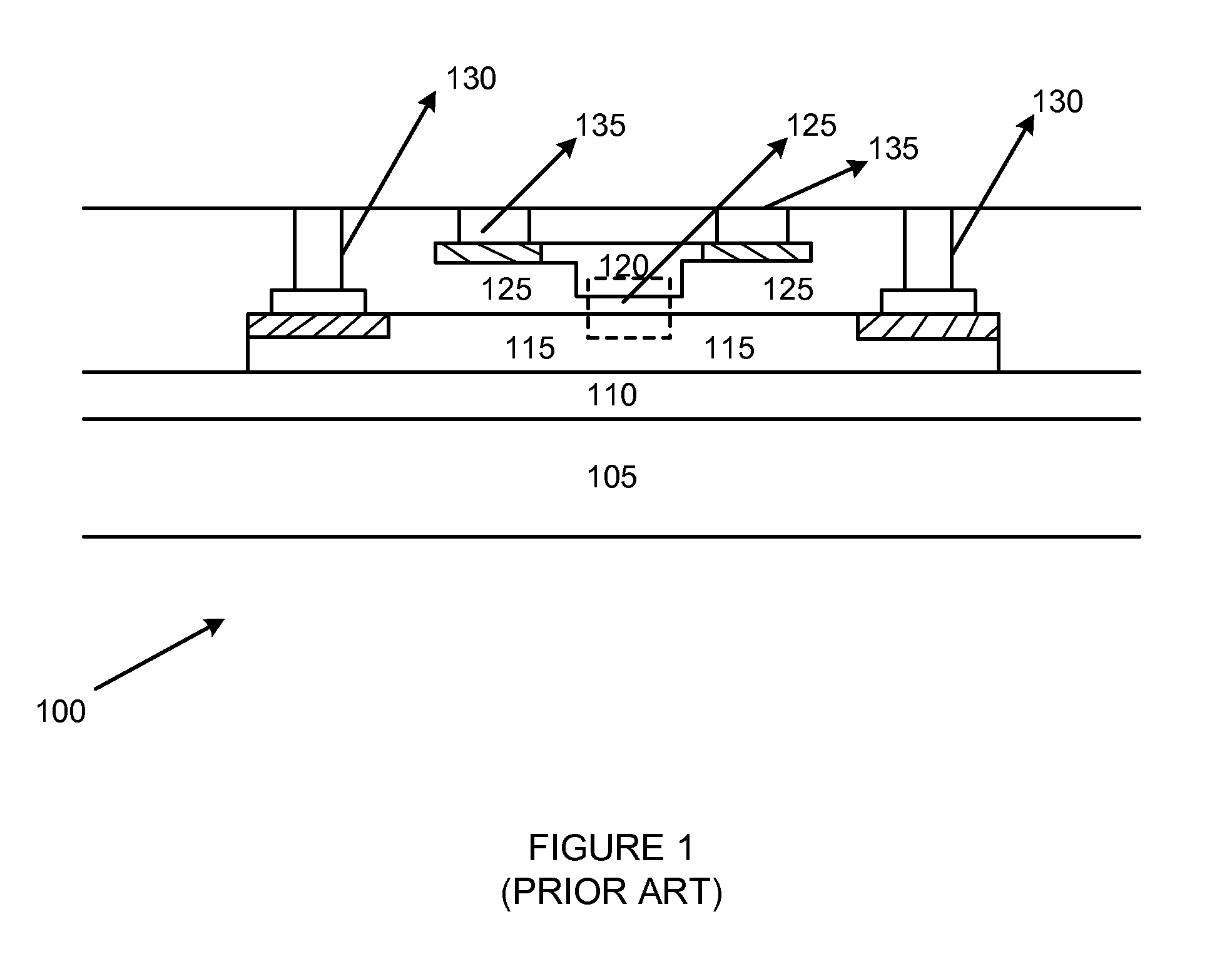
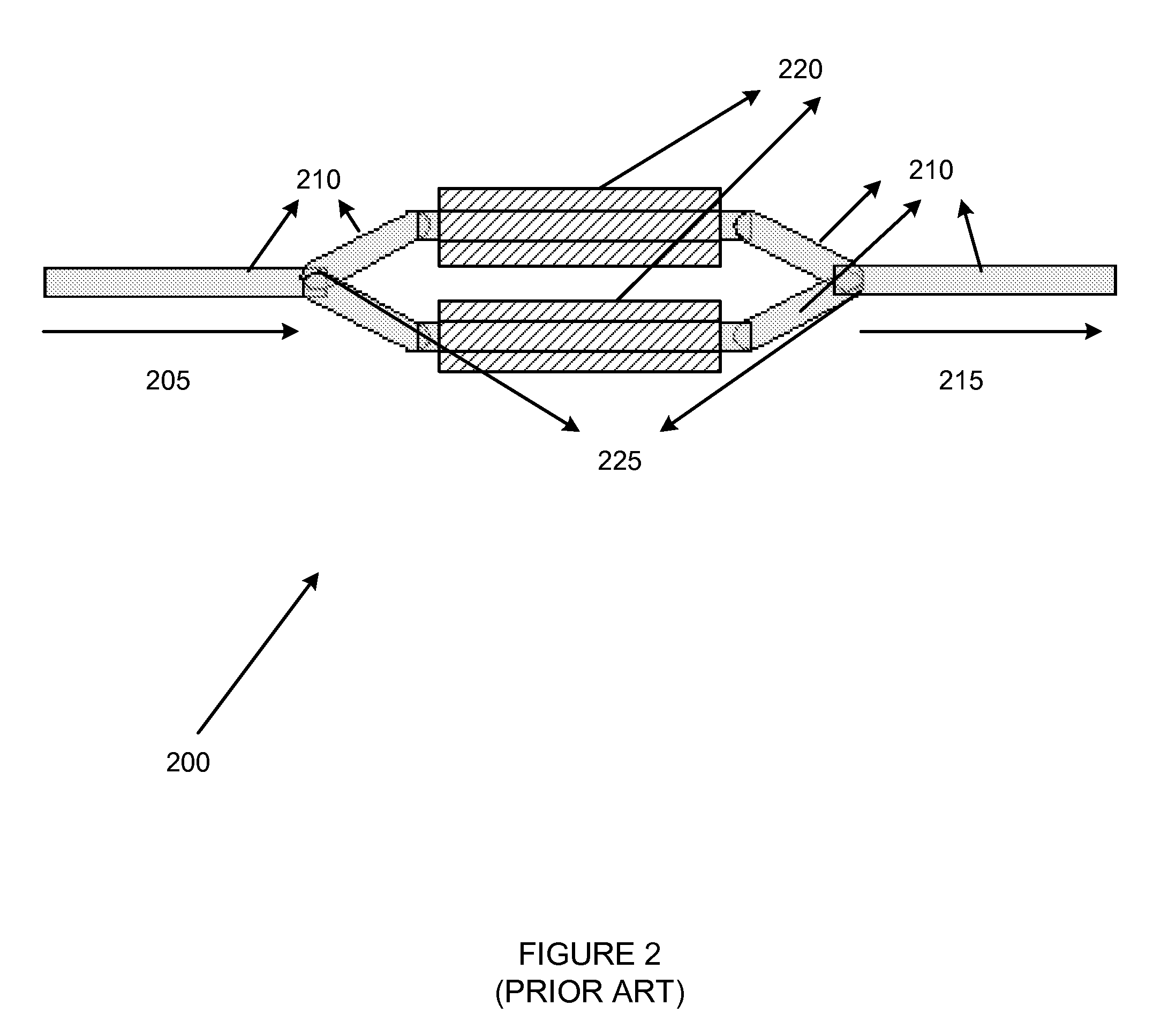
a photonic device and waveguide technology, applied in the direction of optical waveguide light guide, optical elements, instruments, etc., can solve the problems of reducing the efficiency of waveguide phase shifters (b>100/b>, b>400/b>) of figs. 1 and 4, and reducing the efficiency of waveguide phase shifters, so as to improve electrical connectivity and minimize optical loss. , the effect of minimizing optical loss

Active Publication Date: 2011-09-06
ORACLE INT CORP
View PDF6 Cites 17 Cited by
  • Summary
  • Abstract
  • Description
  • Claims
  • Application Information

AI Technical Summary

Benefits of technology

[0029]In general, in one aspect, embodiments of the invention relate to a method of improving electrical connectivity and minimizing optical loss in a photonic waveguide structure. The method includes providing an electrical contact on top of a semiconductor photonic waveguide, said electrical contact being formed of a material with an optical refractive index close to that of a surrounding oxide layer that surrounds the semiconductor waveguide and the electrical contact and lower than the optical refractive index of constituent semiconductor layers. The electrical contact minimizes optical loss by isolating a propagating optical mode between a core of the semiconductor waveguide and a metal electrode contacting said electrical contact.

Problems solved by technology

With high performance computing (HPC) entering into the multi-core Central Processing Unit (CPU) era and linear scaling of computing bandwidth with the number of cores, communication bandwidth per core on multi-chips is becoming a performance bottleneck.
Although the abovementioned waveguide phase shifter 100 largely avoids optical absorption by metal, the presence of many defects in the material lattice of poly-Si adds to the lossy nature of the structure, aided by a significant overlap of the optical mode with poly-Si.
Additionally, the efficiency of both the waveguide phase shifters (100, 400) of FIGS. 1 and 4 is compromised due to the presence of lateral electrical contacts instead of contacts on top of the Si optical waveguide.
Again, this causes the structure to be lossy as there is significant overlap of the optical mode 650 with the metal.
However, a compromise between conductivity and transparency has to be reached during film deposition, as a high concentration of charge carriers will increase the conductivity of the material but decrease the transparency of the material.

Method used


Image

  • Electrical contacts on top of waveguide structures for efficient optical modulation in silicon photonic devices
  • Electrical contacts on top of waveguide structures for efficient optical modulation in silicon photonic devices
  • Electrical contacts on top of waveguide structures for efficient optical modulation in silicon photonic devices

Examples


Embodiment Construction

[0046]Specific embodiments of the invention will now be described in detail with reference to the accompanying figures. Like elements in the various figures are denoted by like reference numerals for consistency.

[0047]In the following detailed description of embodiments of the invention, numerous specific details are set forth in order to provide a more thorough understanding of the invention. However, it will be apparent to one of ordinary skill in the art that the invention may be practiced without these specific details. In other instances, well-known features have not been described in detail to avoid unnecessarily complicating the description.

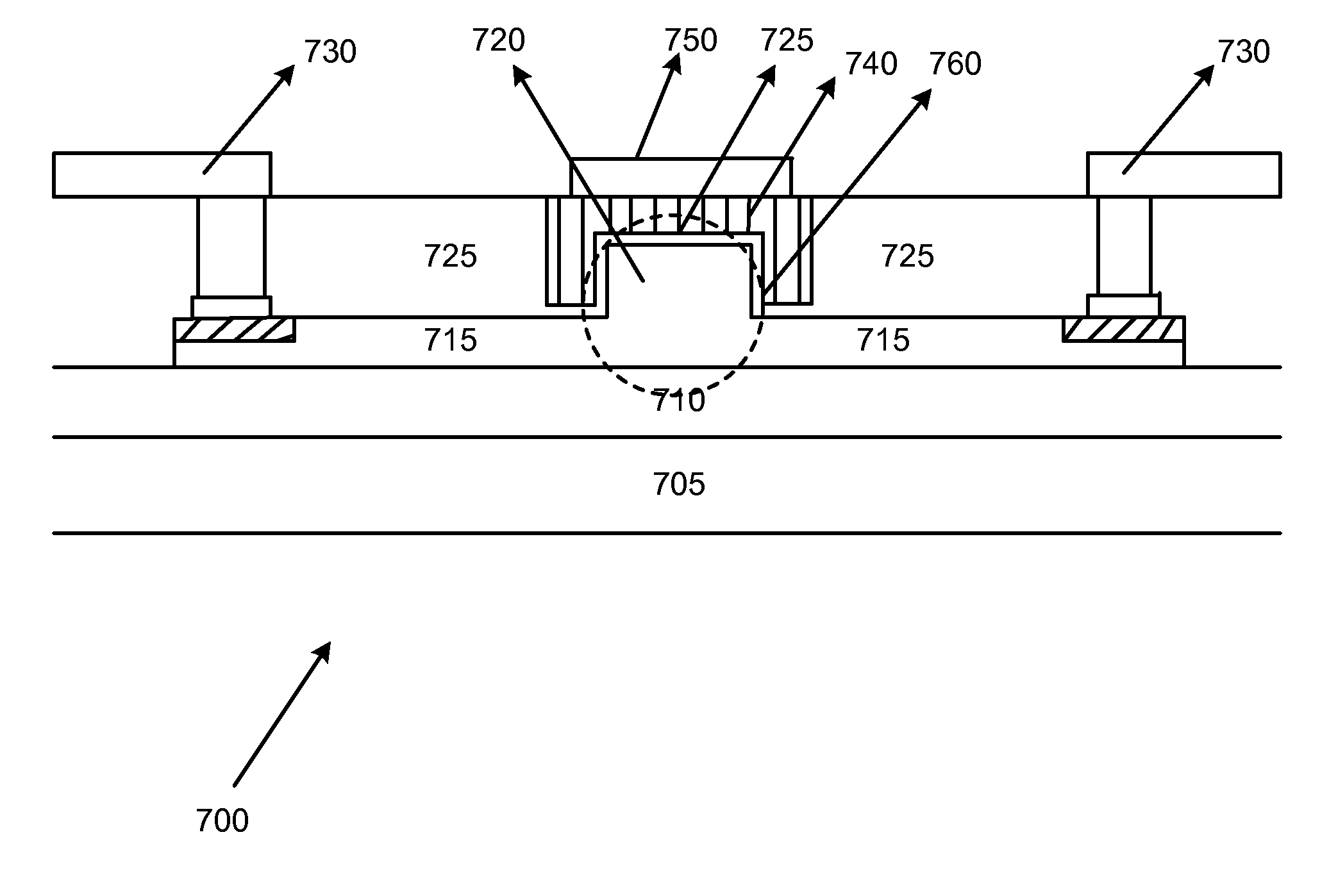
[0048]In general, embodiments of the present invention describe a photonic waveguide structure with an improved conductive electrical contact on top of the waveguide for reduced optical loss in high-speed optical modulators. In one or more embodiments, such an electrical contact may isolate the propagating mode between the waveguide core a...


PUM

PropertyMeasurementUnit
widthsaaaaaaaaaa
optical wavelengthaaaaaaaaaa
voltageaaaaaaaaaa

Abstract

A phase modulation waveguide structure includes one of a semiconductor and a semiconductor-on-insulator substrate, a doped semiconductor layer formed over the one of a semiconductor and a semiconductor-on-insulator substrate, the doped semiconductor portion including a waveguide rib protruding from a surface thereof not in contact with the one of a semiconductor and a semiconductor-on-insulator substrate, and an electrical contact on top of the waveguide rib. The electrical contact is formed of a material with an optical refractive index close to that of a surrounding oxide layer that surrounds the waveguide rib and the electrical contact and lower than the optical refractive index of the doped semiconductor layer. During propagation of an optical mode within the waveguide structure, the electrical contact isolates the optical mode between the doped semiconductor layer and a metal electrode contact on top of the electrical contact.

Description

STATEMENT REGARDING FEDERALLY SPONSORED RESEARCH OR DEVELOPMENT[0001]The U.S. Government has a paid-up license in this invention and the right in limited circumstances to require the patent owner to license others on reasonable terms as provided for by the terms of Agreement No. HR0011-08-9-001 awarded by DARPA.BACKGROUND OF INVENTION[0002]1. Field of the Invention[0003]The invention relates generally to photonic waveguide structures with improved electrical contacts for reducing lossy performance during optical modulation in high-speed optical modulators. More specifically, the invention relates to a photonic waveguide structure, where the provision of a conductive electrical contact isolates a propagating optical mode between the waveguide core and the electrodic contact while maintaining excellent electrical connectivity and low optical loss.[0004]2. Background Art[0005]The tunable non-linear optical properties of Silicon (Si) have been a major factor in the recent emergence of S...

Claims


Application Information

Patent Timeline
Patent Type & Authority Patents(United States)
IPC IPC(8): G02F1/035H01L29/06H04B10/04
CPCB82Y20/00G02F1/01708G02F1/025G02F2001/0157G02F2201/12G02F1/0157Y10S977/742
Inventor SHUBIN, IVANLI, GUOLIANGCUNNINGHAM, JOHN E.KRISHNAMOORTHY, ASHOKZHENG, XUEZHE
Owner ORACLE INT CORP
Why Eureka
Try Eureka