Field emission device

a field emission and emission device technology, applied in the manufacture of electric discharge tubes/lamps, discharge tubes luminescnet screens, instruments, etc., can solve the problems of high manufacturing cost, environmental pollution, non-uniform emission, etc., to improve the emission uniformity of the phosphor layer, high efficiency emission, and high voltage

Active Publication Date: 2011-09-13
ELECTRONICS & TELECOMM RES INST
View PDF8 Cites 24 Cited by
  • Summary
  • Abstract
  • Description
  • Claims
  • Application Information

AI Technical Summary

Benefits of technology

[0020]By the above method, when trajectories of the electron beams emitted from the emitters are rapidly changed over time by a voltage difference between the gate electrodes, an electron beam-scanned area can be expanded due to residual images and the electron beam can be more uniformly emitted due to an electron beam scattering effect and a linear beam spreading effect, resulting in improved emission uniformity of the phosphor layer. By using the insulator in which the height from the emitter to the gate electrode is greater than the diameter of the gate opening, a high voltage can be applied to the anode substrate, thereby attaining high efficiency emission.

Problems solved by technology

The disadvantages include high manufacturing cost, environmental pollution, and nonuniform emission in, for example, a large display device.
However, arc discharge occurring in a free space between the cathode substrate 140 and the anode substrate 110 makes it difficult to apply a high voltage to the anode electrode 120, thus degrading fluorescence efficiency.
Accordingly, it is difficult to attain complete triode operation and apply a high anode voltage, as in the diode type.
However, the increased number of the openings 190 or the field emitters 160 makes it difficult to attain process yield and uniform arrangement of the emitters.
Furthermore, because the distance between the anode substrate 110 and the cathode substrate 140 cannot increase indefinitely due to structural limitations, it is difficult to obtain a highly uniform emission characteristic.

Method used


Image

  • Field emission device
  • Field emission device
  • Field emission device

Examples


Embodiment Construction

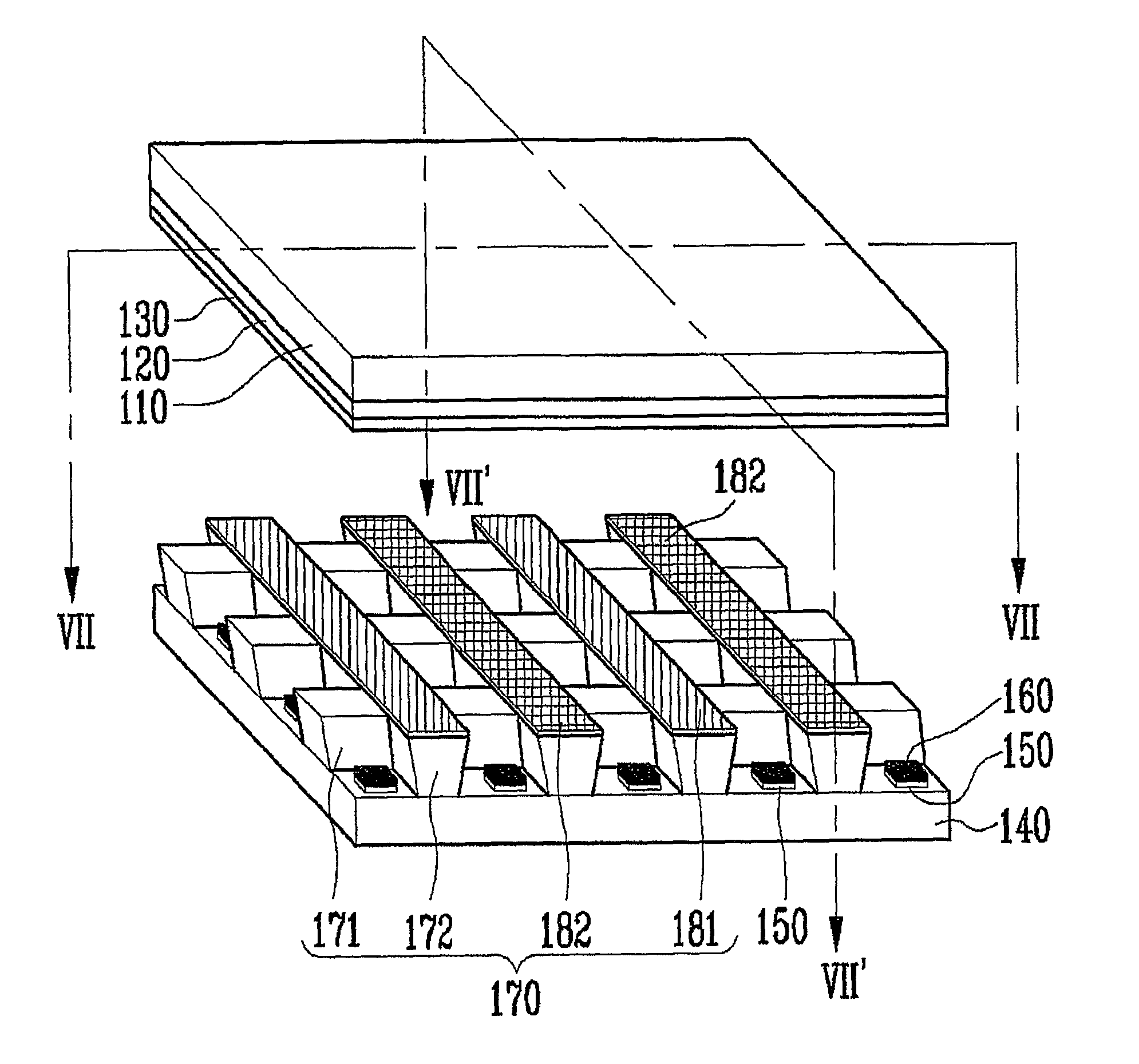
[0053]Hereinafter, exemplary embodiments of the present invention will be described in detail. In the present exemplary embodiment, a gate insulator has a height greater than that of a gate electrode to form a gate substrate having a height greater than a diameter of an opening. However, to increase the height of the gate substrate, the gate electrode may have a greater thickness. In this manner, the height of the gate substrate may increase by increasing either the height of the gate insulator or the height of the gate electrode.

[0054]FIG. 5 is a partially enlarged perspective view schematically illustrating a field emission device according to an exemplary embodiment of the present invention, FIG. 6 is an enlarged plan view of an area of a cathode substrate of FIG. 5, and FIG. 7 is a cross-sectional view taken along line VII-VII of FIG. 5.

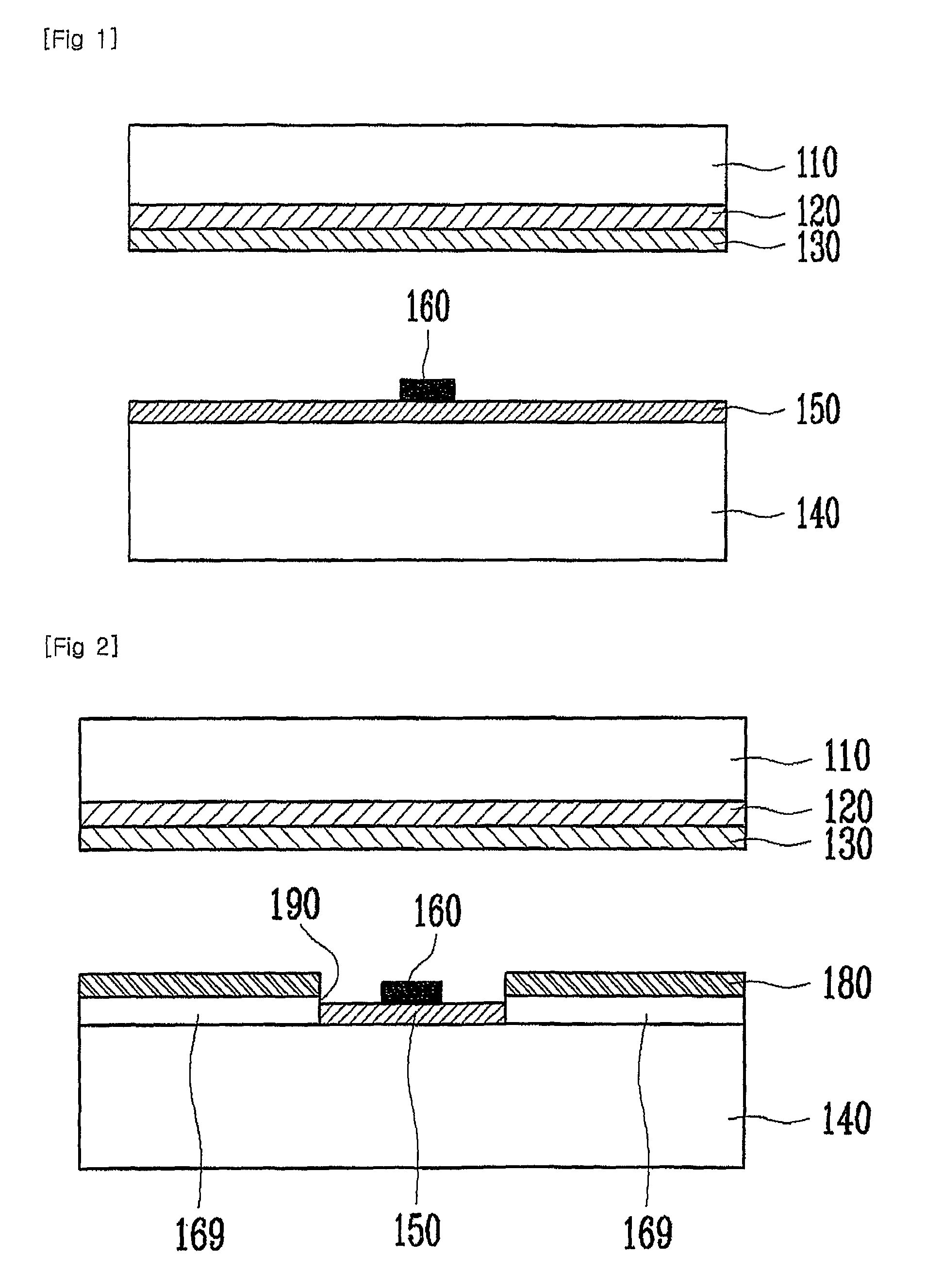
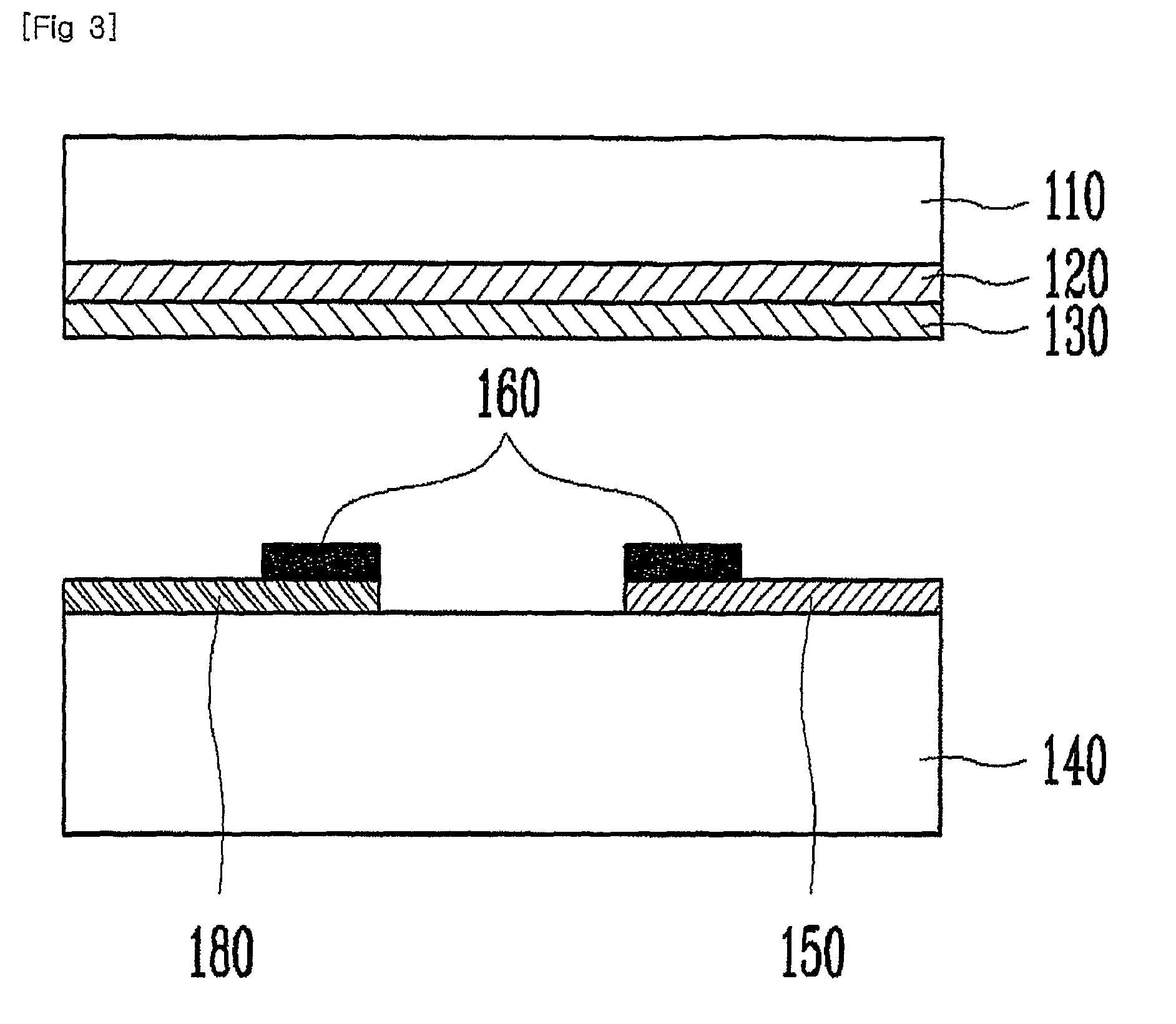
[0055]Referring to FIGS. 5 to 7, the present field emission device, i.e., a field emission backlight unit includes an anode substrate 110, a cat...


PUM


Abstract

Disclosed is a field emission device. The field emission device includes: an anode substrate including an anode electrode formed on a surface thereof and a fluorescent layer formed on the anode electrode; a cathode substrate disposed opposite to and spaced apart from the anode substrate, and including at least one cathode electrode formed toward the anode substrate and a field emitter formed on each cathode electrode; and a gate substrate having one surface in contact with the cathode substrate, wherein the gate substrate include gate insulators surrounding the field emitters and having a plurality of openings exposing the field emitters, and a plurality of gate electrodes formed on the gate insulators around the openings and electrically isolated from one another. Thus, when the trajectories of the electron beams emitted from the emitters are rapidly changed over time by a voltage difference between the gate electrodes, an electron beam-scanned area can be expanded due to residual images and the electron beam can be more uniformly emitted due to an electron beam scattering effect and a linear beam spreading effect, resulting in improved emission uniformity of the fluorescent layer.

Description

TECHNICAL FIELD[0001]The present invention relates to a field emission device, and more particularly, to a field emission device capable of attaining a high efficiency emission characteristic using a field emission lamp having a structure in which a plurality of gate electrodes are electrically isolated.BACKGROUND ART[0002]In general, a field emission device emits light using cathodoluminescence in a fluorescent layer on an anode substrate by causing electrons emitted from a field emitter on a cathode substrate to collide with the fluorescent layer. Here, the cathode substrate is disposed opposite to and spaced apart from the anode substrate by a specific distance, and the substrates are vacuum-packaged. Recently, a field emission lamp has been studied and developed as an alternative to a backlight unit for a conventional liquid crystal display (LCD), a flat light device, and a typical illumination device. In particular, the backlight unit generally includes a cold cathode fluoresce...

Claims


Application Information

Patent Timeline
Patent Type & Authority Patents(United States)
IPC IPC(8): H01J1/30H01J1/304
CPCH01J1/304H01J63/06H01J9/148H01J2201/30469H01J2203/026
Inventor JEONG, JIN WOOSONG, YOON HOKIM, DAE JUN
Owner ELECTRONICS & TELECOMM RES INST
Why Eureka
Try Eureka