Vertically integrated 3-axis MEMS accelerometer with electronics

a technology of accelerometer and electronics, applied in the field of accelerometers, can solve the problems of increasing the cost, affecting the accuracy of the accelerometer, so as to reduce the complexity of the sense electronics, reduce the sensitivity to packaging and temperature changes, and reduce the mechanical nois

Active Publication Date: 2011-11-01
INVENSENSE
View PDF188 Cites 66 Cited by
  • Summary
  • Abstract
  • Description
  • Claims
  • Application Information

AI Technical Summary

Benefits of technology

Acceleration sensing in each axis is achieved by separate structures where the motion of the proof mass affects the value of sense capacitor. Two structures can be used per axis to enable full bridge measurements to further reduce the mechanical noise, susceptibility to power supply changes, cross axis coupling and the complexity of the sense electronics. To reduce the sensitivity to packaging and temperature changes, each mechanical structure is anchored to a single anchor pillar bonded to the top cover.

Problems solved by technology

For example, there are contradicting requirements over the area (cost) of the accelerometer and the noise performance.
Therefore, building heavy proof masses requires relatively large area which in return increases the cost.
Surface micromachining also necessitates complex fabrication steps.
Moreover, non-uniformity of the deposited films and large variation of the material properties have negative impact on the process yield and cost.
Controlling stress level in the film is another issue which needs to be dealt with otherwise undesired curling of the released structures may occur.
In addition, moveable parts released by using sacrificial wet etching may suffer from the stiction problem if their mechanical properties are not selected properly.
But this adversely affects the sensitivity of the accelerometer where the sensitivity is inversely proportional to the resonant frequency.
Therefore, stiction problem limits the accelerometer sensitivity.
In addition to above described technical difficulties, surface micromachining tools are not readily available to small companies.
Most of the required equipment can only be supported by a complicated infrastructure that only large companies can afford.
This sets a very high barrier for small start-up companies that want to enter the accelerometer market.
Surface micromachining is not a feasible solution for companies which do not have access to the expensive fabrication equipment.

Method used


Image

  • Vertically integrated 3-axis MEMS accelerometer with electronics
  • Vertically integrated 3-axis MEMS accelerometer with electronics
  • Vertically integrated 3-axis MEMS accelerometer with electronics

Examples


Embodiment Construction

The present invention relates generally to motion sensing devices and more specifically to accelerometers utilized in integrated circuits. The following description is presented to enable one of ordinary skill in the art to make and use the invention and is provided in the context of a patent application and its requirements. Various modifications to the preferred embodiments and the generic principles and features described herein will be readily apparent to those skilled in the art. Thus, the present invention is not intended to be limited to the embodiments shown, but is to be accorded the widest scope consistent with the principles and features described herein.

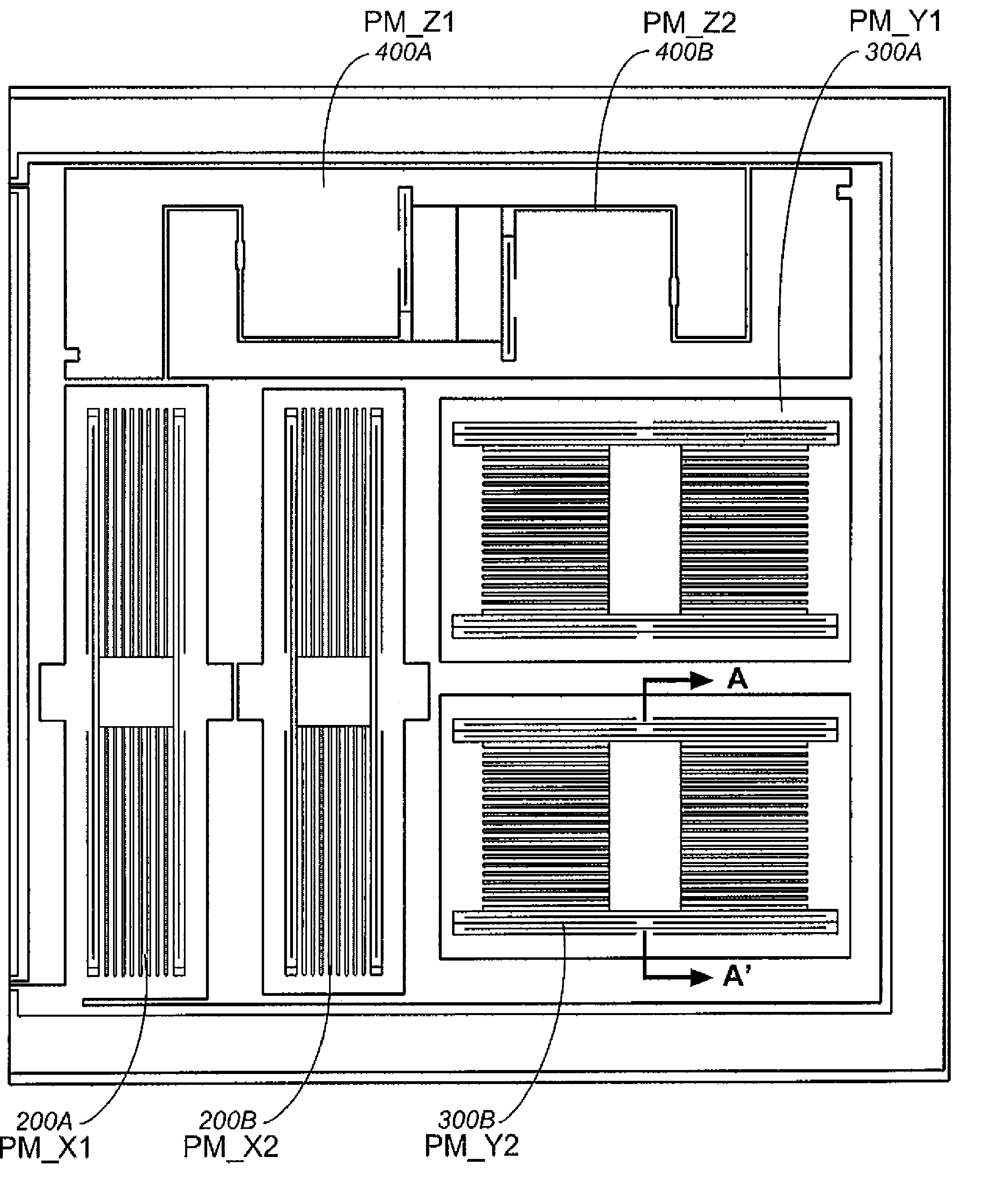
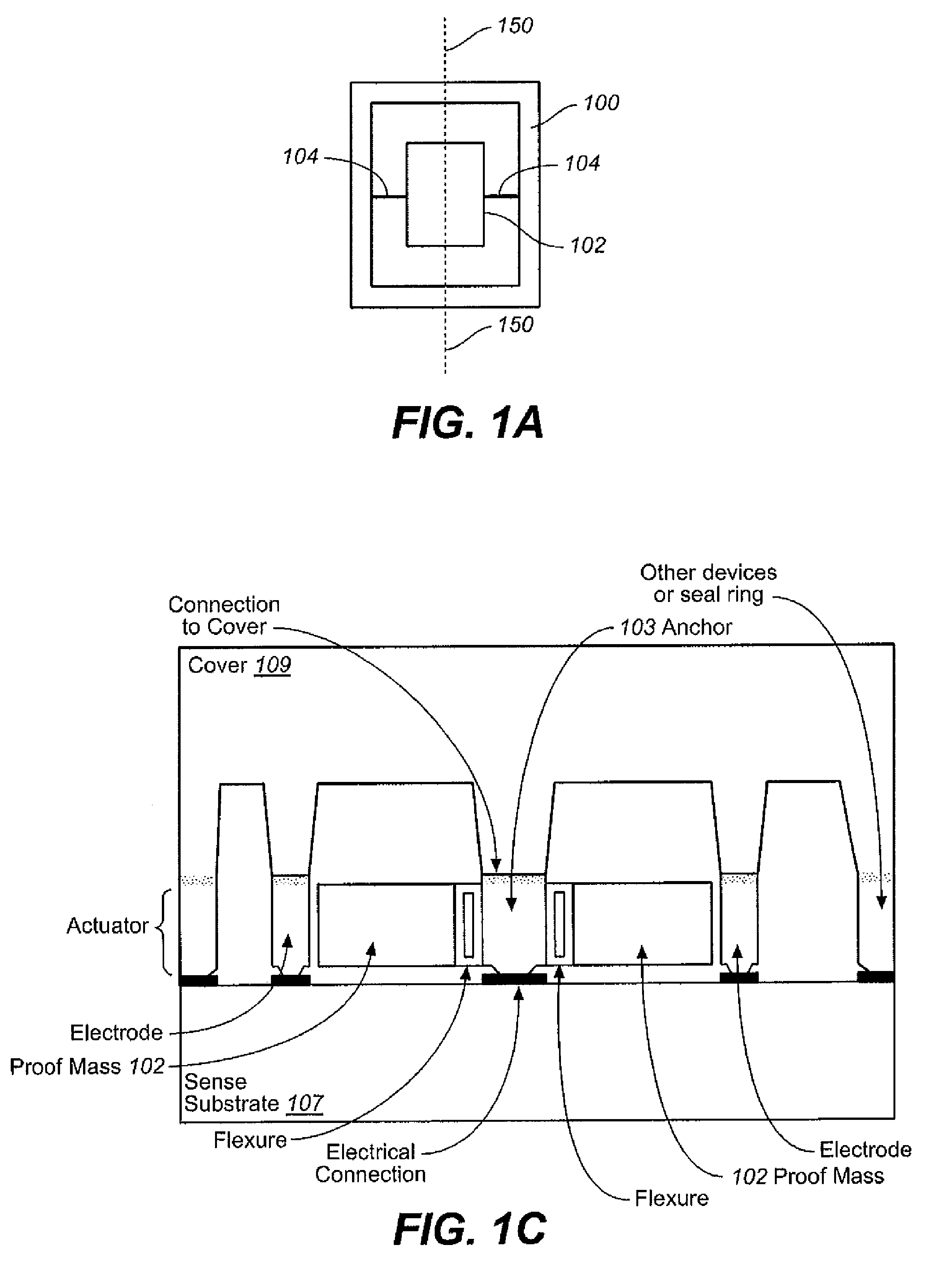
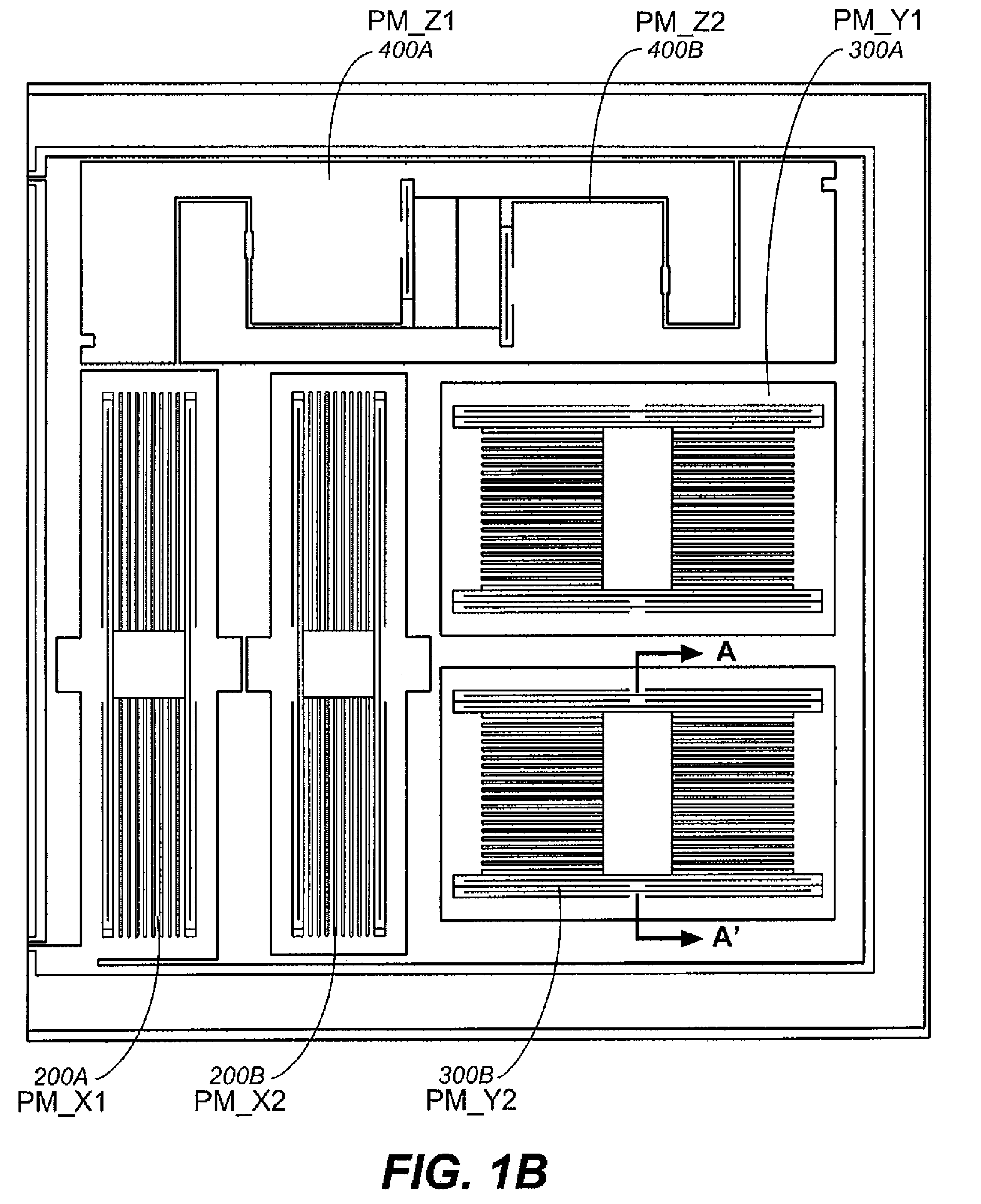
A method and system in accordance with the present invention relates to the accelerometers that are fabricated using silicon micromachining methods that have been described in U.S. Pat. No. 6,892,575, entitled “X-Y axis dual-mass tuning fork gyroscope with vertically integrated electronics and wafer-scale hermetic packagi...


PUM


Abstract

A system and method in accordance with the present invention provides for a low cost, bulk micromachined accelerometer integrated with electronics. The accelerometer can also be integrated with rate sensors that operate in a vacuum environment. The quality factor of the resonances is suppressed by adding dampers. Acceleration sensing in each axis is achieved by separate structures where the motion of the proof mass affects the value of sense capacitors differentially. Two structures are used per axis to enable full bridge measurements to further reduce the mechanical noise, immunity to power supply changes and cross axis coupling. To reduce the sensitivity to packaging and temperature changes, each mechanical structure is anchored to a single anchor pillar bonded to the top cover.

Description

FIELD OF THE INVENTIONThe present invention relates generally to motion sensing devices and more specifically to accelerometers that are utilized in integrated circuits.BACKGROUND OF THE INVENTIONAccelerometers are widely used for motion sensing applications. Conventionally, an accelerometer consists of a suspended proof mass and a means of measuring the proof mass displacement with respect to the reference frame. Recent advances in microelectronics technology enabled fabrication of accelerometers with integrated electronics in volume production. One of the first applications of these integrated micromachined sensors was in airbag deployment for automobiles (Analog Device's XL50).The first accelerometer products that were fabricated using MEMS technology were introduced by large corporations such as Analog Devices, ST and Bosch who had already infrastructure to produce integrated circuits. Integrated circuit fabrication mostly involves depositing several dielectric layers and select...

Claims


Application Information

Patent Timeline
Patent Type & Authority Patents(United States)
IPC IPC(8): G01P15/125
CPCG01P15/125G01P15/18G01P2015/0814G01P2015/0831
Inventor NASIRI, STEVEN S.SEEGER, JOSEPHYARALIOGLU, GOKSEN
Owner INVENSENSE
Why Eureka
Try Eureka