Peeling method

a technology of semiconductor devices and peeling methods, which is applied in the direction of semiconductor devices, semiconductor/solid-state device details, electrical apparatus, etc., can solve the problems of unsuitable mass production, cracking of integrated circuits formed by thin films over substrates, etc., and achieve the effect of efficient peeling and easy picking up

Inactive Publication Date: 2011-11-15
SEMICON ENERGY LAB CO LTD
View PDF32 Cites 25 Cited by
  • Summary
  • Abstract
  • Description
  • Claims
  • Application Information

AI Technical Summary

Benefits of technology

[0022]In accordance with the present invention, a separating layer (also referred to as a peeling layer) is damaged at a plurality of times by at least two different kinds of methods (a damage due to laser light irradiation, a damage due to etching, or a damage due to a physical means), subsequently, the layer to be peeled can be efficiently separated (also referred to as peeled) from a substrate. By damaging at a plurality of times by using at least two different kinds of methods, a synergistic effect of peeling far easier than the case of using one peeling method is obtained. Since peeling can be far easier than the case of using one peeling method, the present invention is suitable for peeling using especially a large substrate.
[0072]In accordance with the present invention, a device on a plane surface can become easy to be picked up by controlling the arch of the device at its initial state.

Problems solved by technology

A semiconductor wafer which is a maternal body of a semiconductor chip used for an IC card or a noncontact IC tag is expensive, and so it is unsuitable for mass-production.
Further, an integrated circuit which is formed by a thin film over a substrate may be cracked when the integrated circuit is peeled from the substrate.

Method used


Image

  • Peeling method
  • Peeling method
  • Peeling method

Examples


embodiment 1

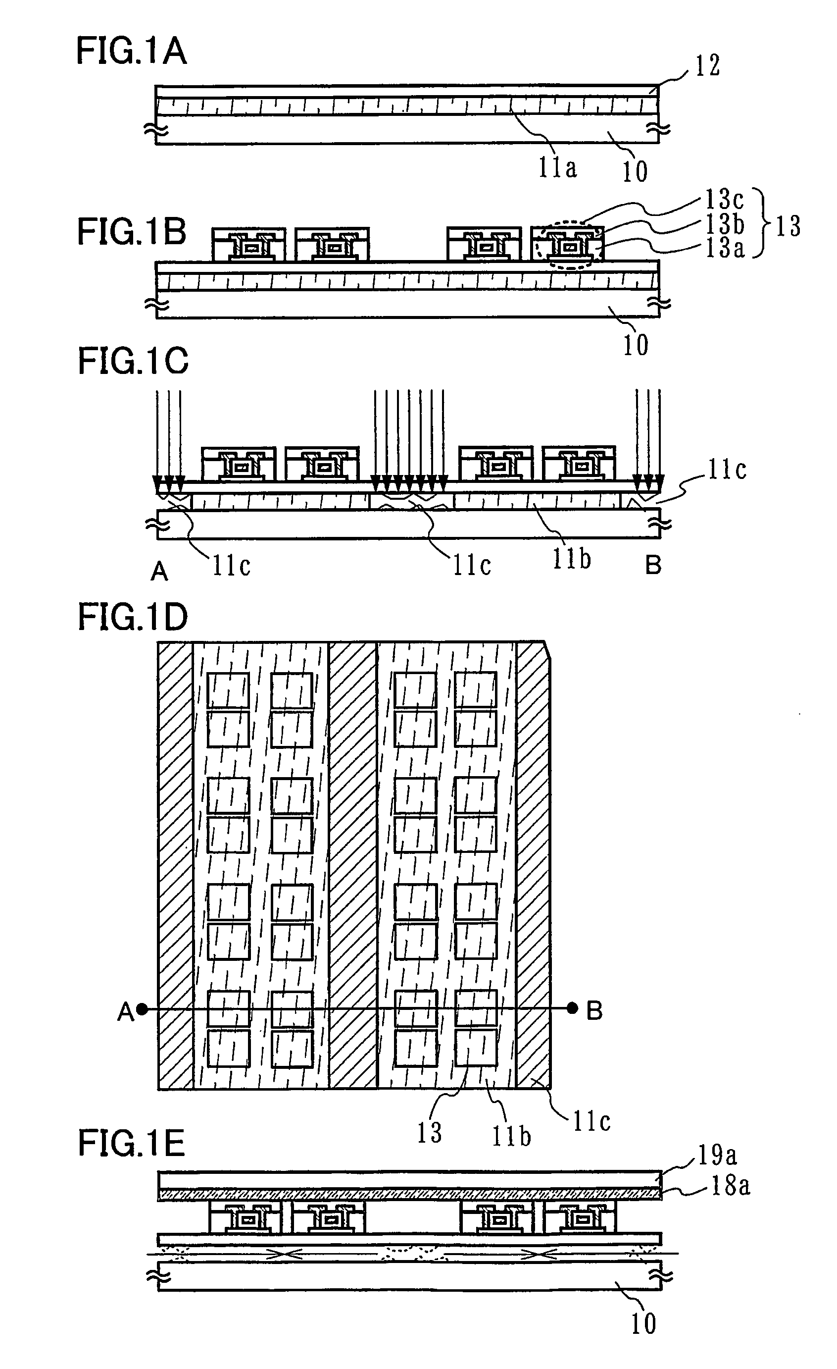
[0085]A method for manufacturing the semiconductor device in accordance with the present invention is explained hereinafter.

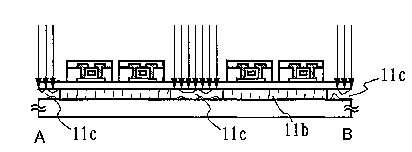
[0086]A separating layer 11a is formed over a substrate having an insulating surface 10. A substrate having an insulating surface 10 corresponds to a glass substrate, a quartz substrate, a plastic substrate, a resin substrate made from synthetic resin having flexibility such as acrylic, or a metal substrate. The separating layer 11a is formed by a layer containing silicon by a known method such as a sputtering method or a plasma CVD method. The layer containing silicon corresponds to an amorphous semiconductor layer, a semiamorphous semiconductor layer in which an amorphous state and a crystalline state are mixed, or a crystalline semiconductor layer.

[0087]A base insulating layer 12 is formed by an inorganic insulating film. As the base insulating layer 12, a single layer film made from silicon oxide, silicon nitride, silicon oxynitride, silicon nitride oxide, ...

embodiment 2

[0103]A manufacturing method which is different from that described in Embodiment 1 is explained with reference to FIGS. 4A to 5B.

[0104]A separating layer 411a is formed over the whole surface of a substrate having an insulating surface 410. Here, a tungsten (W) film obtained by a sputtering method is used as the separating layer. Then, a base insulating layer 412a is formed by an inorganic insulating film (refer to FIG. 4A). As a material for the base insulating layer 412a, a material which hardly reacts or does not react chemically with gas or liquid containing fluorine halide used in the subsequent process is preferably used. The base insulating layer 412a is preferably formed by a laminated layer of silicon oxide film or a silicon nitride film. Here, a silicon nitride film is stacked over a silicon oxide film which is in contact with the tungsten film.

[0105]A layer to be peeled 413 using a base insulating film 412a as a base film is formed. The layer to be peeled including a fir...

embodiment 3

[0129]An example of manufacturing apparatus for a thin film integrated circuit is explained in this embodiment.

[0130]FIG. 6A shows manufacturing apparatus which arches the device by means of laminating in accordance with Embodiment 1.

[0131]The manufacturing apparatus shown in FIG. 6A has a delivery roller for a film 1401, a take-up roller for a film 1402, transporting rollers 1403, 1404, a substrate carrier arm 1409, and rollers 1410, 1411.

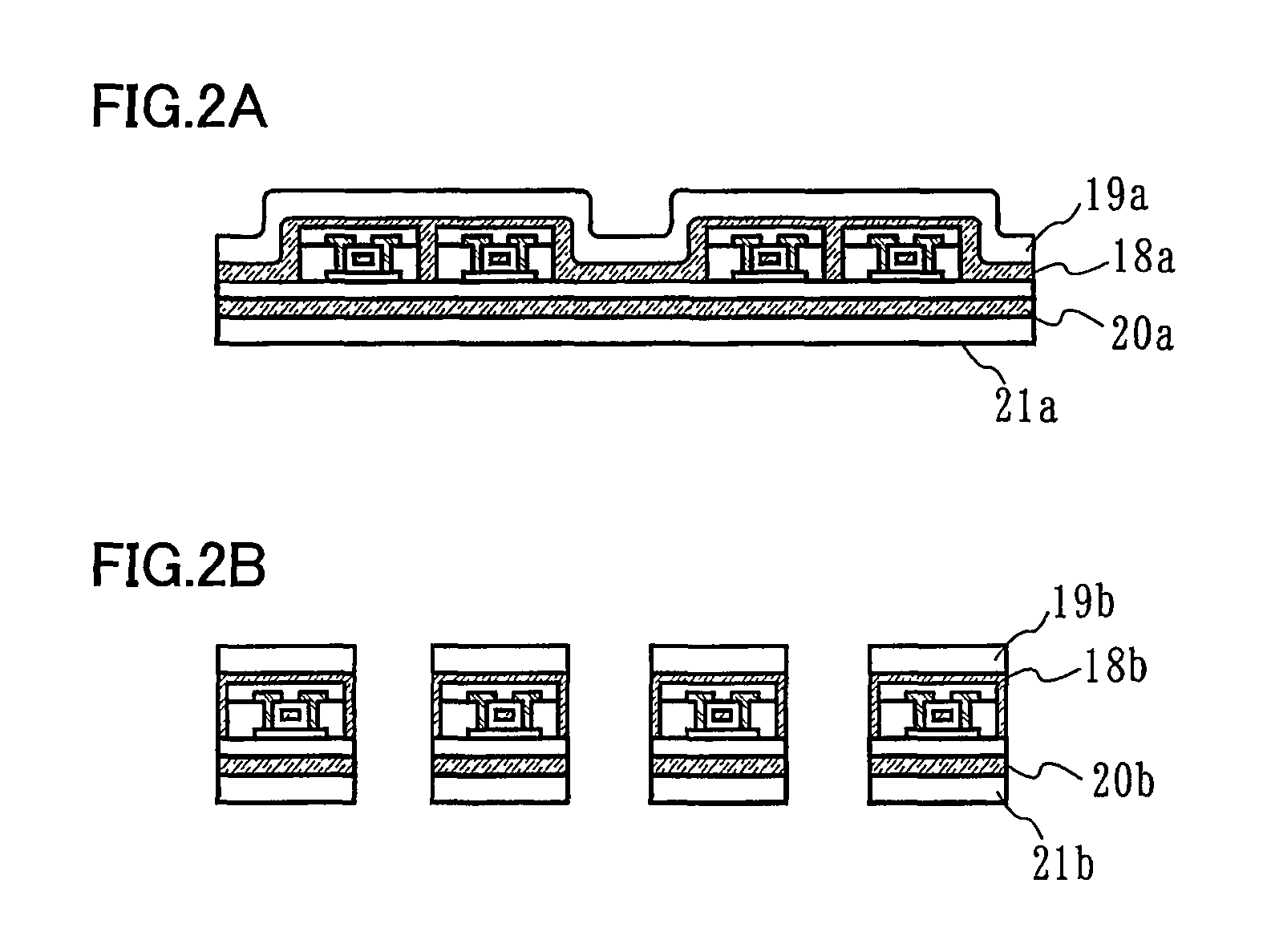
[0132]In accordance with Embodiment 1, the state shown in FIG. 1E is obtained, and a first film 19a is held by the substrate carrier arm 1409 with a vacuum chuck. Like components are denoted by like numerals as of Embodiment 1. The first film 19a is provided with a first adhesion layer 18a. A layer including an antenna 1408 is adhered to a layer including a TFT 1407 by the first adhesion layer 18a.

[0133]The first film 19a is simply mounted over the laminate film by lightly pressing the first film 19a at the laminated film which is delivered from ...


PUM


Abstract

The present invention provides a method for manufacturing massively and efficiently a minute device which can receive or send data in contact, preferably, out of contact by forming an integrated circuit which is formed by a thin film over a large glass substrate and by peeling the integrated circuit from the substrate. Especially, an integrated circuit which is formed by a thin film is extremely thin, and so there is a threat that the integrated circuit is flied when transporting, and so handling thereof is difficult. In accordance with the present invention, a separating layer (also referred to as a peeling layer) is damaged at a plurality of times by at least two different kinds of methods (a damage due to laser light irradiation, a damage due to etching, or a damage due to a physical means), subsequently, the layer to be peeled can be efficiently peeled from a substrate. Further, handling of individual devices becomes easy by arching the peeled device.

Description

TECHNICAL FIELD[0001]The present invention relates to a semiconductor device having a circuit constructed by a thin film transistor (hereinafter, TFT) and a method for manufacturing the semiconductor device. For example, the present invention relates to an electric appliance which is mounted with a light-emitting display device having an electro-optical device or an organic light-emitting element as a component.[0002]In this specification, the term “semiconductor device” refers to a device in general which can operate by utilizing semiconductor characteristics. An electro-optical device, a semiconductor circuit, and an electric appliance are semiconductor devices.BACKGROUND ART[0003]In recent years, a technique of constructing a thin film transistor (TFT) with a semiconductor thin film (with a thickness of approximately several to several hundreds nm) formed over a substrate having an insulating surface has attracted attention. The thin film transistor is widely used in an electroni...

Claims


Application Information

Patent Timeline
Patent Type & Authority Patents(United States)
IPC IPC(8): H01L21/84H01L25/00
CPCH01L27/13H01L27/1214H01L27/1266H01L2924/3511
Inventor KUWABARA, HIDEAKI
Owner SEMICON ENERGY LAB CO LTD
Why Eureka
Try Eureka