Packaging substrate structure and manufacturing method thereof

a technology of packaging substrate and manufacturing method, applied in the direction of electrical apparatus construction details, association of printed circuit non-printed electric components, printed element electric connection formation, etc., can solve the problems of poor electrical connection, poor impedance control, and rather difficult processing, so as to prevent poor electrical connection and poor impedance control

Active Publication Date: 2011-11-15
UNIMICRON TECH CORP
View PDF16 Cites 5 Cited by
  • Summary
  • Abstract
  • Description
  • Claims
  • Application Information

AI Technical Summary

Benefits of technology

[0014]According to the above drawbacks, an objective of the present invention is to provide a packaging substrate structure and a manufacturing method thereof so as to prevent the conventional drawback of insufficient thickness or a hollow center of a large-dimension conductive block that results in an uneven thickness of the circuit layer.
[0015]Another objective of the present invention is to provide a packaging substrate structure and a manufacturing method thereof so as to facilitate a subsequent circuit built-up process and via processing and prevent poor electrical connection and poor impedance control.
[0030]Since the large-dimension first circuit layer has a plurality of dielectric pillars, the difference of the electric current density distribution between the large-dimension opening area and the small-dimension opening areas during electroplating can be reduced so as to prevent insufficient thickness or a hollow center of the conductive block that results in an uneven thickness of the circuit layer, thereby facilitating via processing in a subsequent circuit built-up process and preventing poor electrical connection and poor impedance control.

Problems solved by technology

As a result, the dielectric layer of the subsequent formed built-up circuit can have an uneven thickness, which makes the via processing rather difficult and accordingly leads to poor electrical connection and poor impedance control.

Method used


Image

  • Packaging substrate structure and manufacturing method thereof
  • Packaging substrate structure and manufacturing method thereof
  • Packaging substrate structure and manufacturing method thereof

Examples


first embodiment

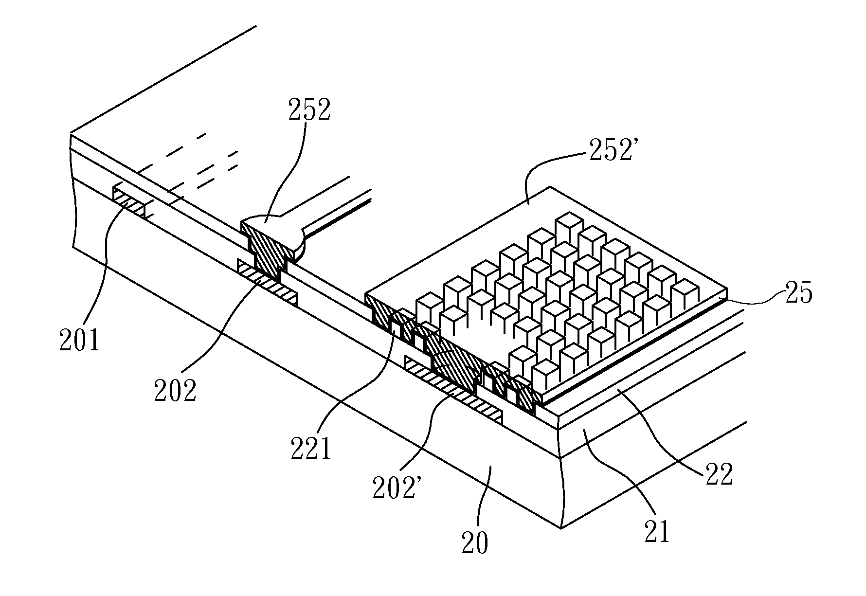
[0038]FIGS. 2A to 2F are views showing a manufacturing method of a packaging substrate structure according to a first embodiment of the present invention.

[0039]As shown in FIG. 2A, a carrier layer 20 is provided, and a patterned circuit layer is disposed on at least a surface of the carrier layer 20, wherein the patterned circuit layer has a plurality of circuits 201 and first electrical connection terminals 202, 202′. The carrier layer 20 is one of a core board and a dielectric layer of a multi-layer packaging substrate. At least a first dielectric layer 21 is formed on the patterned circuit layers 201, 202, 202′ and at least a surface of the carrier layer 20. A plurality of first vias 210, 210′ are formed in the first dielectric layer 21, allowing surfaces of the first electrical connection terminals 202, 202′ to be exposed from the first vias 210, 210′.

[0040]As shown in FIG. 2B, a second dielectric layer 22 is formed on the first dielectric layer 21. A plurality of small-dimensio...

second embodiment

[0047]FIGS. 3A to 3D are cross-sectional views showing a manufacturing method of a packaging substrate structure according to a second embodiment of the present invention. The second embodiment is different from the first embodiment in that the first and second circuit layers of the second embodiment are formed through a full additive process.

[0048]As shown in FIG. 3A, a structure similar to that of FIG. 2B is shown. A patterned circuit layer is disposed on the surface of a carrier layer 30. The patterned circuit layer comprises a plurality of circuits 301 and first electrical connection terminals 302, 302′. The carrier layer 30 is one of a core board and a dielectric layer of a multi-layer packaging substrate. A first dielectric layer 31 is formed on the surfaces of the carrier layer 30 and the patterned circuit layers 301, 302, 302′. A plurality of first vias 310, 310′ are formed in the first dielectric layer 31 to expose a portion of the first electrical connection terminals 302,...


PUM

PropertyMeasurementUnit
dielectricaaaaaaaaaa
conductiveaaaaaaaaaa
dimensionaaaaaaaaaa

Abstract

A packaging substrate structure includes a dielectric layer with a plurality of dielectric pillars disposed on a portion of a large-dimension opening area of the dielectric layer; and a first circuit layer with a plurality of first circuits disposed on a portion of the dielectric layer, and a conductive block disposed in the large-dimension opening area of the dielectric layer having the dielectric pillars. The dielectric pillars reduce the difference of the electrical current density distribution between the large-dimension opening area and small-dimension opening areas during electroplating, thereby overcoming the conventional drawback of insufficient thickness or a hollow center of the conductive block that results in an uneven thickness of the circuit layer. The invention further provides a method of manufacturing the packaging substrate structure.

Description

BACKGROUND OF THE INVENTION[0001]1. Field of the Invention[0002]The present invention relates generally to a packaging substrate structure and a manufacturing method thereof, and more particularly, to a packaging substrate structure, circuit layer of which has a large-dimension conductive block, and a manufacturing method of the packaging substrate structure.[0003]2. Description of Related Art[0004]Owing to the flourishing development of the electronics industry, the research and development of electronic products have a trend toward multi-function, high-performance products. To satisfy the packaging requirements of high integration and miniaturization for semiconductor packages, multi-layer packaging substrates are developed, wherein dielectric layers and circuit layers are formed on the surface of a core substrate, and conductive vias are formed in the dielectric layers for electrical connection between the circuit layers.[0005]Besides general circuits, circuits of a multi-layer p...

Claims


Application Information

Patent Timeline
Patent Type & Authority Patents(United States)
IPC IPC(8): H05K1/00H05K3/42
CPCH05K1/116H05K3/423H05K3/421H05K3/465Y10T29/49165H05K2201/09036H05K2201/09563H05K2201/096H05K2201/0373
Inventor HSU, SHIH-PING
Owner UNIMICRON TECH CORP
Why Eureka
Try Eureka