Aluminum copper oxide based memory devices and methods for manufacture

a memory device and copper oxide technology, applied in the direction of bulk negative resistance effect devices, transistors, instruments, etc., can solve the problems of increasing the complexity of the circuitry of memory devices employing these types of materials, increasing the power consumption of memory devices, and relatively slow programming speeds, etc., to reduce power consumption during programming of memory elements described herein, the effect of low programming voltag

Active Publication Date: 2011-11-29
MACRONIX INT CO LTD
View PDF11 Cites 103 Cited by
  • Summary
  • Abstract
  • Description
  • Claims
  • Application Information

AI Technical Summary

Benefits of technology

[0009]Advantageously, anti-fuse metal-oxide memory elements comprising aluminum oxide and copper oxide as described herein are shown to have a relatively low programming voltage (for example 6 Volts) and a fast programming time (for example 30 nsec). As a result, the power consumption during programming of the memory elements described herein is reduced compared to other types of anti-fuse based memory. Additionally, the memory elements described herein are shown to have a large resistance ratio between the high and low resistance states and exhibit very good data retention in both states.
[0010]Memory arrays having memory cells as described herein result in high density memory. In embodiments the cross-sectional area of the memory cells of the array can be determined entirely by dimensions of the word lines and bit lines, allowing for a high memory density for the array. The word lines have word line widths and adjacent word lines are separated by a word line separation distance, and the bit lines have bit line widths and adjacent bit lines are separated by a bit line separation distance. In some embodiments the sum of the word line width and the word line separation distance is equal to twice a feature size F used to form the array, and the sum of the bit line width and the bit line separation distance is equal to twice the feature size F. Additionally, F can be a minimum feature size for a process (typically a lithographic process) used to form the bit lines and word lines, such that memory cells of the array have a memory cell area of 4F2.

Problems solved by technology

Typically programming voltages of 10 V or more are needed, which increases the complexity of circuitry for memory devices employing these types of materials.
In addition, the breakdown process can take a relatively long time (for example greater than 1 microsecond) and require a large current, resulting in relatively slow programming speeds and high power consumption.

Method used


Image

  • Aluminum copper oxide based memory devices and methods for manufacture
  • Aluminum copper oxide based memory devices and methods for manufacture
  • Aluminum copper oxide based memory devices and methods for manufacture

Examples


first embodiment

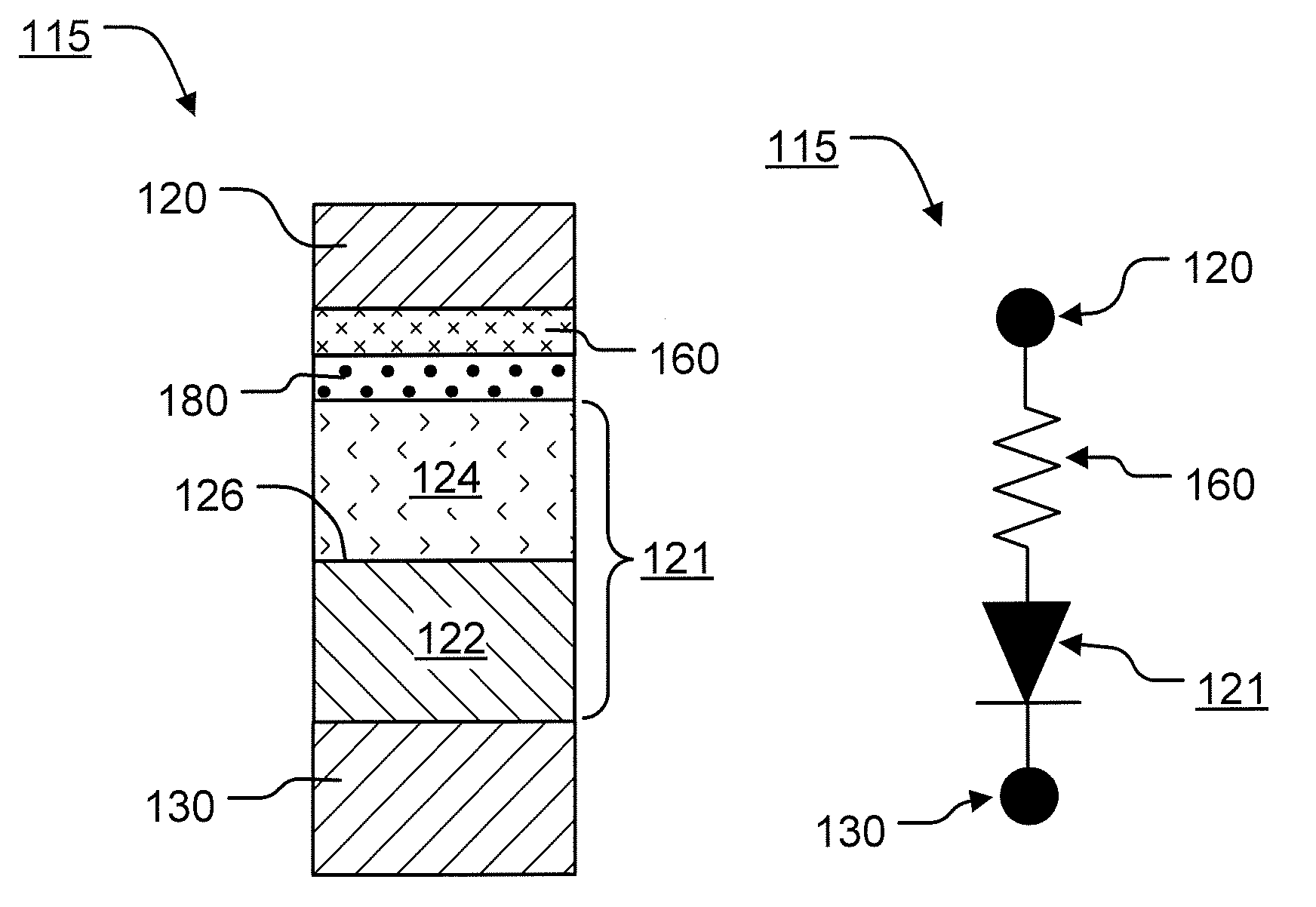
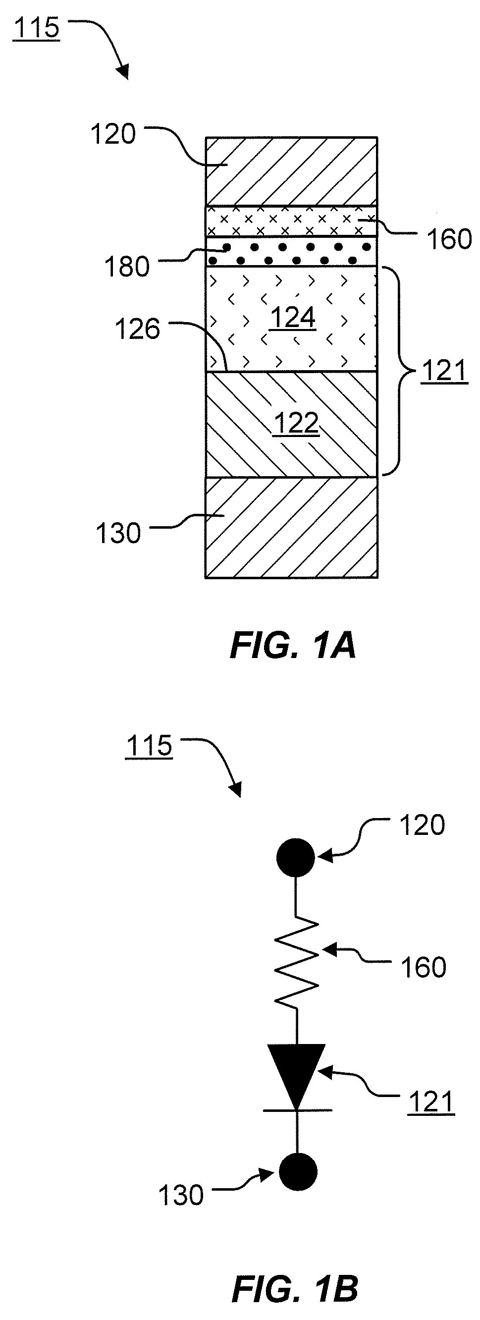
[0025]FIG. 1A illustrates a cross-sectional view of a memory cell 115 including an anti-fuse metal-oxide memory element 160 comprising aluminum and copper. The memory cell 115 includes a diode 121 arranged in electrical series with the memory element 160 along a current path between a first electrode 130 and a second electrode 120. FIG. 1B illustrates a schematic diagram of the memory cell 115 of FIG. 1A.

[0026]The first and second electrodes 130, 120 are conductive elements respectively. The first and second electrodes 130, 120 may each comprise, for example, one or more elements selected from the group consisting of Ti, W, Mo, Al, Ta, Cu, Pt, It, La, Ni, N, O, and Ru and combinations thereof, and in some embodiments may comprise more than one layer. In some embodiments the first electrode 130 may comprise a portion of a word line, and the second electrode 120 may comprise a portion of a bit line.

[0027]The memory cell 115 includes a conductive element 180 between the memory element ...

second embodiment

[0044]In the illustrated embodiment of FIG. 1A the memory element 160 overlies the diode 121. FIG. 5A illustrates a cross-sectional view of a second embodiment for the memory cell 115 with the diode 121 overlying the memory element 160. FIG. 5B illustrates a schematic diagram of the memory cell 115 of FIG. 5A. The same reference numbers for the various elements are used in FIGS. 5A-5B as in FIGS. 1A-1B.

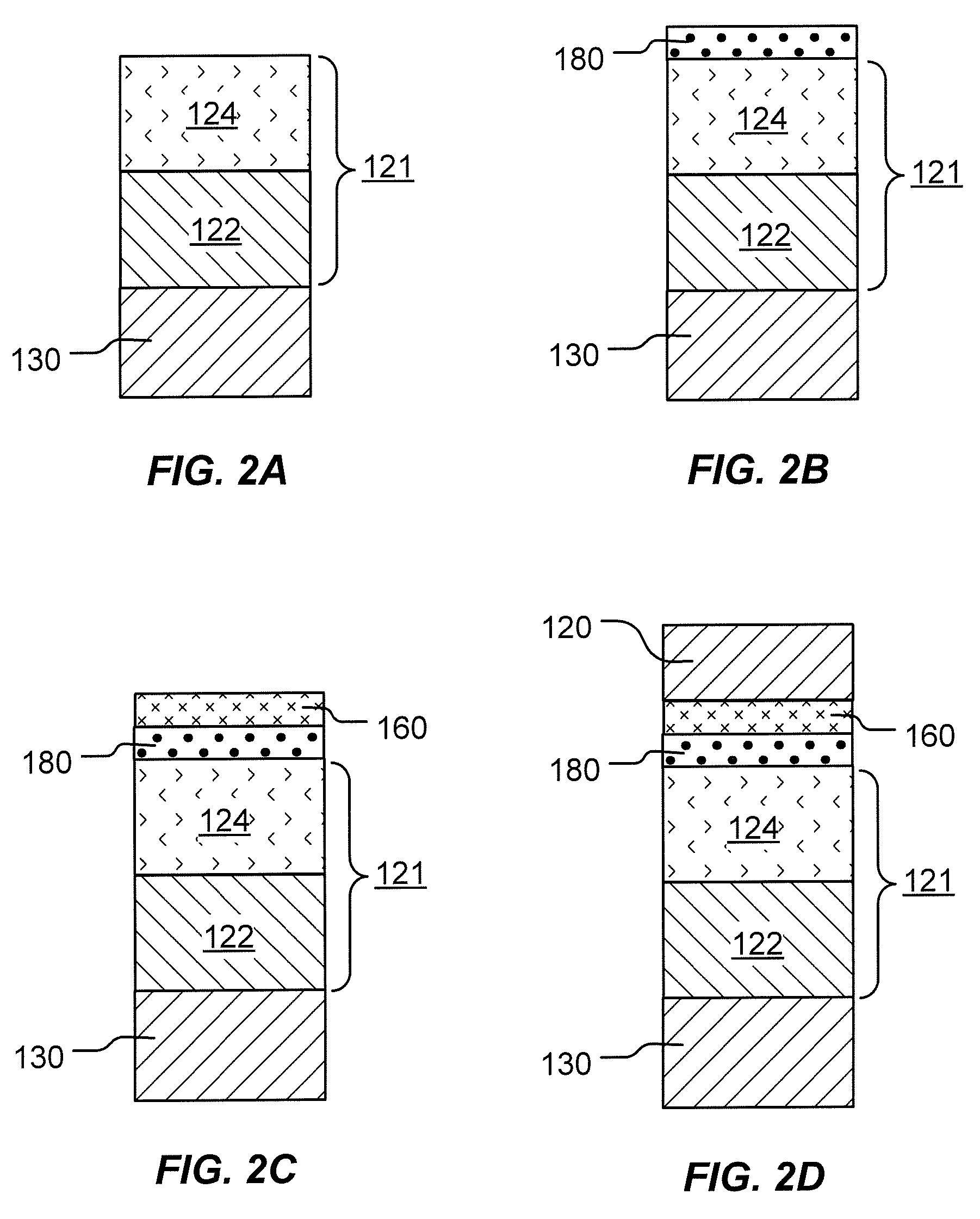
[0045]FIGS. 6A-6D illustrate steps in a manufacturing process for manufacturing the memory cell 115 of FIG. 5A. The materials and processes discussed above with respect to FIGS. 1A-1B and 2A-2D can be used in the various steps of FIGS. 6A-6D, and thus a detailed description is not repeated here.

[0046]FIG. 6A illustrates a first step of forming the conductive element 180 on the bottom electrode 130. Next, the memory element 160 is formed on the conductive element 180, resulting in the structure illustrated in the cross-sectional view of FIG. 6B. The diode 121 is then formed on the memo...


PUM


Abstract

Memory devices are described along with methods for manufacturing. A memory device as described herein includes a first electrode and a second electrode. The memory device further includes a diode and an anti-fuse metal-oxide memory element comprising aluminum oxide and copper oxide. The diode and the metal-oxide memory element are arranged in electrical series between the first electrode and the second electrode.

Description

BACKGROUND OF THE INVENTION[0001]1. Field of the Invention[0002]The present invention relates to metal-oxide based memory devices.[0003]2. Description of Related Art[0004]One-time programmable (OTP) memory is used in integrated circuits for a variety of nonvolatile memory applications. OTP memory is typically implemented using charge storage, fuse, or anti-fuse techniques.[0005]Anti-fuse type memory is programmed by applying a voltage pulse across a dielectric or other high resistance material to induce breakdown and form a low resistance current path through the material. Various materials including silicon oxide, silicon nitride, silicon-oxynitride, aluminum oxide, and hafnium oxide have been proposed for use in anti-fuse type memory. Typically programming voltages of 10 V or more are needed, which increases the complexity of circuitry for memory devices employing these types of materials. In addition, the breakdown process can take a relatively long time (for example greater than...

Claims


Application Information

Patent Timeline
Patent Type & Authority Patents(United States)
IPC IPC(8): H01L29/72
CPCG11C17/16H01L27/1021H01L27/101
Inventor CHIEN, WEI-CHIHCHANG, KUO-PINCHEN, YI-CHOULAI, ERH-KUNHSIEH, KUANG-YEU
Owner MACRONIX INT CO LTD
Why Eureka
Try Eureka