Semiconductor memory device having DRAM-compatible addressing mode and data processing system including same
- Summary
- Abstract
- Description
- Claims
- Application Information
AI Technical Summary
Benefits of technology
Problems solved by technology
Method used
Image

Examples
first embodiment
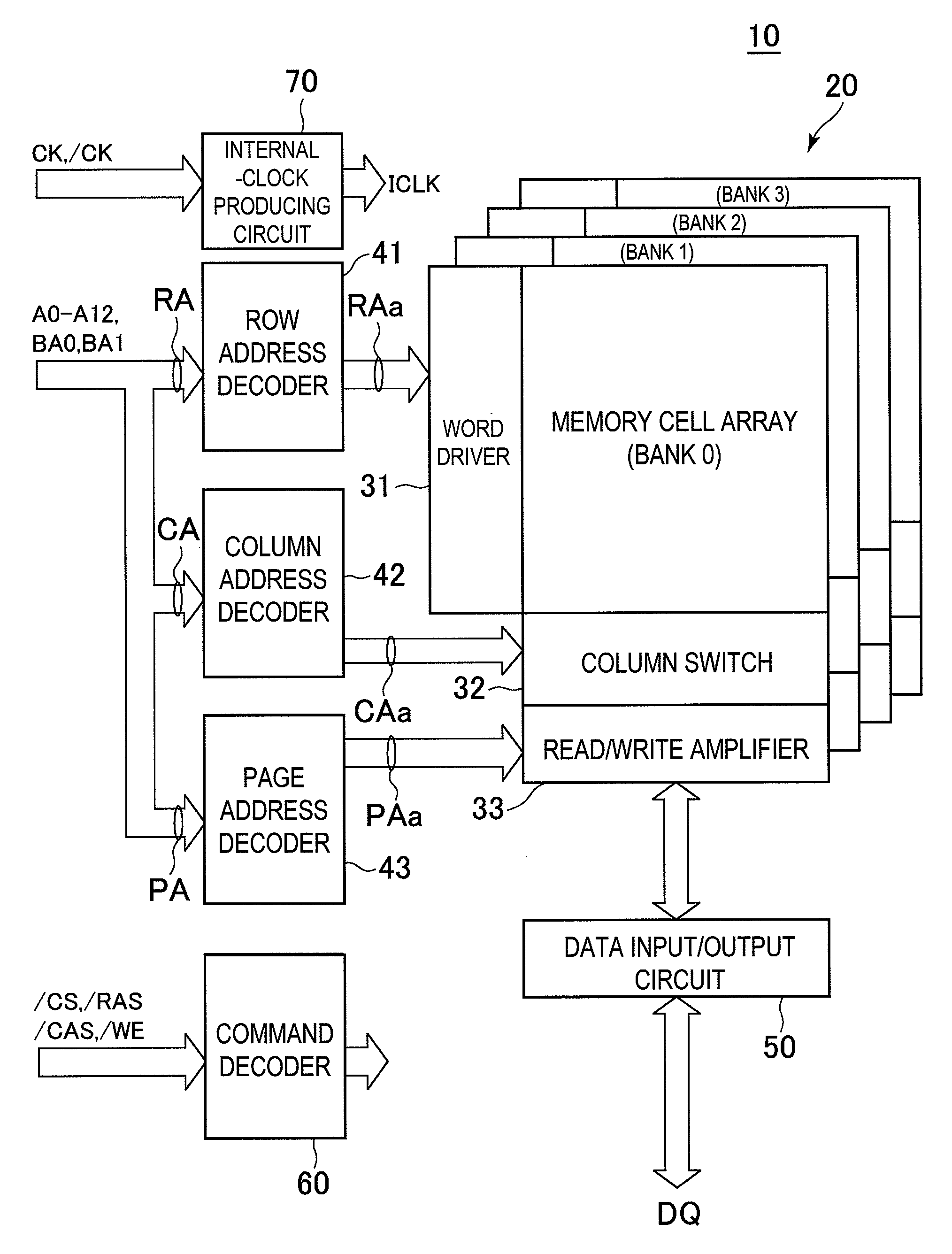
[0034]In the first embodiment, the word driver 31, the column switch 32, and the decoders 41 to 43 configure an address selecting circuit with respect to the memory cell array 20.
[0035]A read data DQ read by the read / write amplifier 33 is output to outside via a data input / output circuit 50. A write data DQ input from outside is supplied to the read / write amplifier 33 via the data input / output circuit 50.
[0036]The active command, the read command, and the write command are expressed by a combination of a chip select signal / CS, a row-address strobe signal / RAS, a column-address strobe signal / CAS, and a write enable signal / WE input from outside, and interpreted by a command decoder 60. A slash ( / ) assigned to the top of reference letter of each signal name means that the signal is low active.
[0037]Each signal (address and command) input from outside, the read data, and the write data DQ are all input and output in synchronism with clock signals CK, and / CK. The clock signals CK and...
second embodiment
[0063]FIG. 7 shows the present invention.
[0064]As shown in FIG. 7, in the second embodiment, each word line is hierarchized into a main word line MWL and a sub word line SWL, and the main word line MWL is shared by the memory cell arrays P0 to P511. The main word line MWL is driven by a main word driver 31M based on a predecode signal RAa1. Moreover, the sub word line SWL is driven by a sub word driver 31S based on a predecode signal RAa2. When such a hierarchized structure is adopted, a circuit scale of the word driver 31 can be significantly downsized.
third embodiment
[0065]FIG. 8 shows the present invention.
[0066]As shown in FIG. 8, in the third embodiment, the sub word driver 31S corresponding to each of the memory cell arrays P0 to P511 is each supplied with a corresponding bit of the decode signal PAa. Other features of the third embodiment are identical to those of the second embodiment shown in FIG. 7, and thus like elements are denoted by like reference numerals, and redundant explanations thereof will be omitted.
[0067]The sub word driver 31S drives the sub word line SWL when the corresponding bit of the decode signal PAa is activated. Therefore, the sub word line SWL is activated in synchronism with the selection of the read / write amplifier 33 by the page address decoder 43 after the page address PA is determined. According to such a configuration, only the sub word driver 31S of the page on which a read operation or a write operation is actually performed is selectively operated, and thus the power consumption can be reduced more as comp...
PUM
 Abstract
Description
Claims
Application Information
 - R&D
- Intellectual Property
- Life Sciences
- Materials
- Tech Scout
- Unparalleled Data Quality
- Higher Quality Content
- 60% Fewer Hallucinations
Browse by: Latest US Patents, China's latest patents, Technical Efficacy Thesaurus, Application Domain, Technology Topic, Popular Technical Reports.
© 2025 PatSnap. All rights reserved.Legal|Privacy policy|Modern Slavery Act Transparency Statement|Sitemap|About US| Contact US: help@patsnap.com