
CMOS microelectromechanical system (MEMS) device and fabrication method thereof

a microelectromechanical and microelectromechanical technology, applied in the direction of fluid pressure measurement, fluid pressure measurement by electric/magnetic elements, instruments, etc., can solve the problems of defect of the mems device, undercutting of the interface between the silicon oxide and the silicon substrate, and damage to the mems structure, etc., to reduce the damage to the diaphragm and reduce the undercut

Active Publication Date: 2012-01-10
SOLID STATE SYST
View PDF5 Cites 10 Cited by
  • Summary
  • Abstract
  • Description
  • Claims
  • Application Information

AI Technical Summary

Benefits of technology

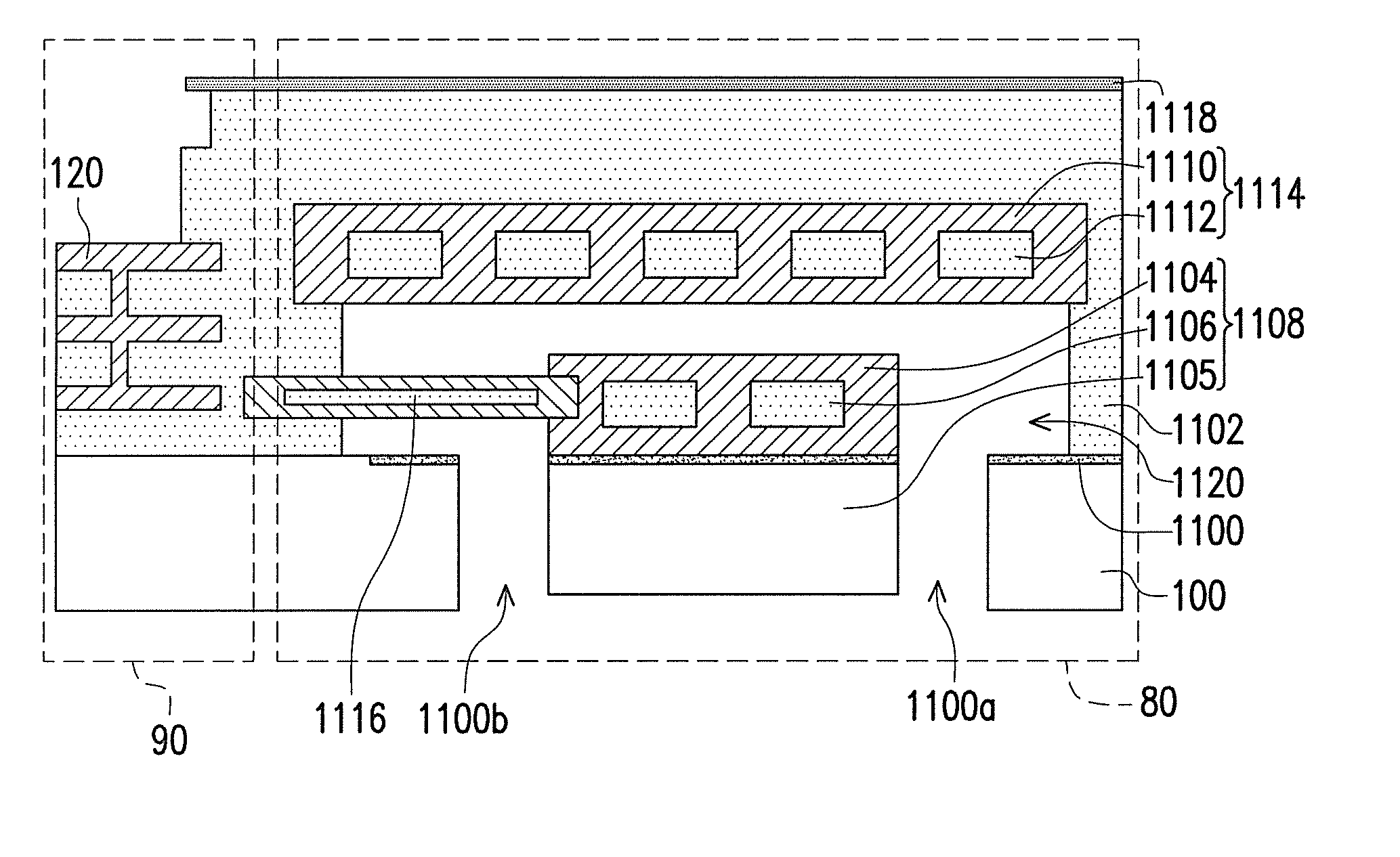
"The invention provides a MEMS device with a CMOS circuit that has a venting hole with reduced undercut and reduced damage to the diaphragm. The method for fabricating the MEMS device includes patterning a substrate from the second side to form a cavity in corresponding to the diaphragm and a plurality of venting holes in the substrate. An isotropic etching process is performed from the first side and the second side of the substrate via the venting holes to remove a dielectric portion of the structural dielectric layer for exposing a central portion of the diaphragm and the back plate while an end portion is held by a residue portion of the structural dielectric layer. The method also includes providing a substrate and forming a metal silicide on the substrate at the first side, covering a MEMS region of the substrate, wherein the metal silicide is exposed in the step of patterning the substrate from the second side to form the isolated silicon bulk."

Problems solved by technology

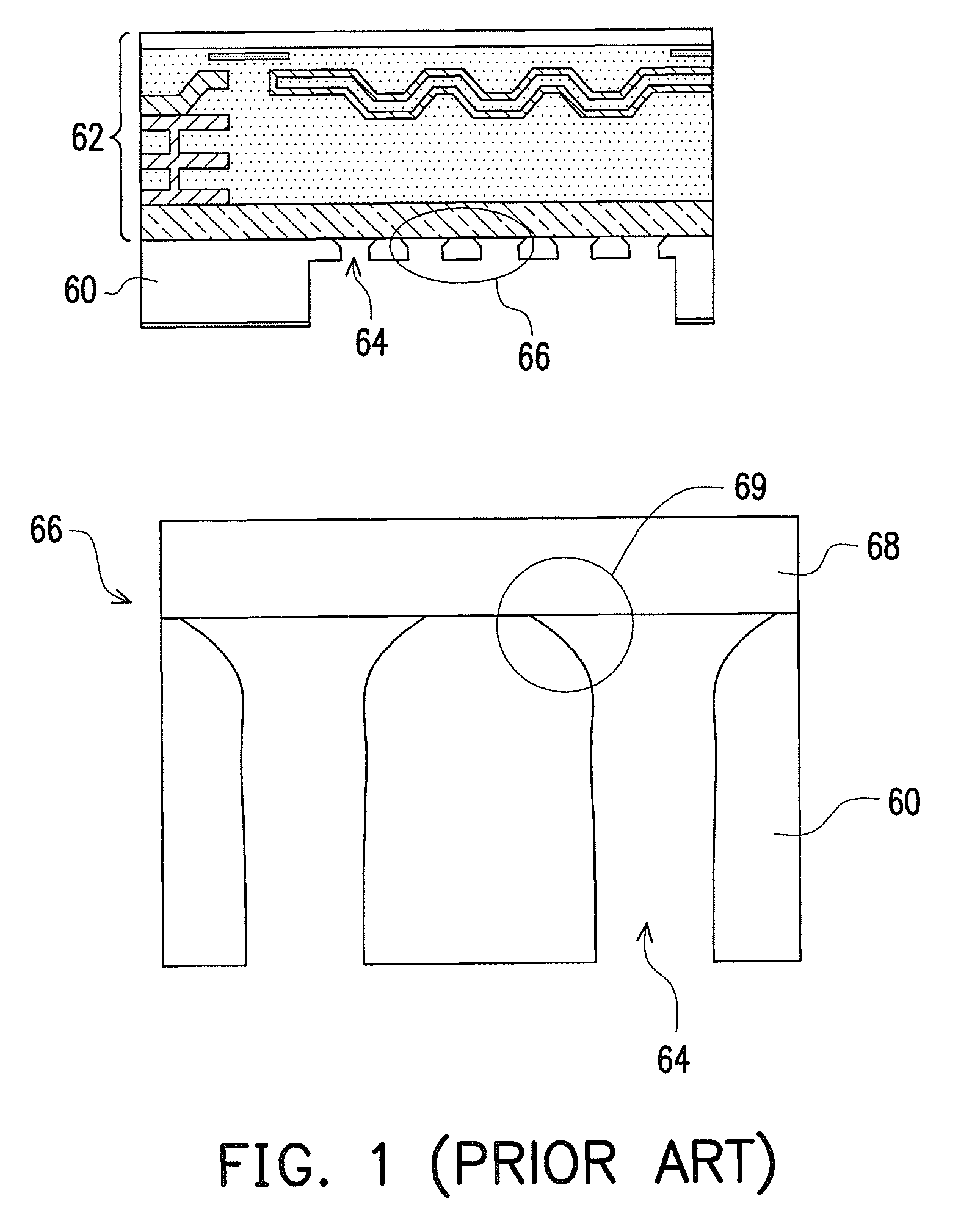
Since the device is under a long time of etching process, the MEMS structure may be damaged.
However, since the depth of venting holes 64 are usually large and need a long etching time, an undercut usually occurs at the interface between the silicon oxide and the silicon substrate 60.
This causes defects of the MEMS device.
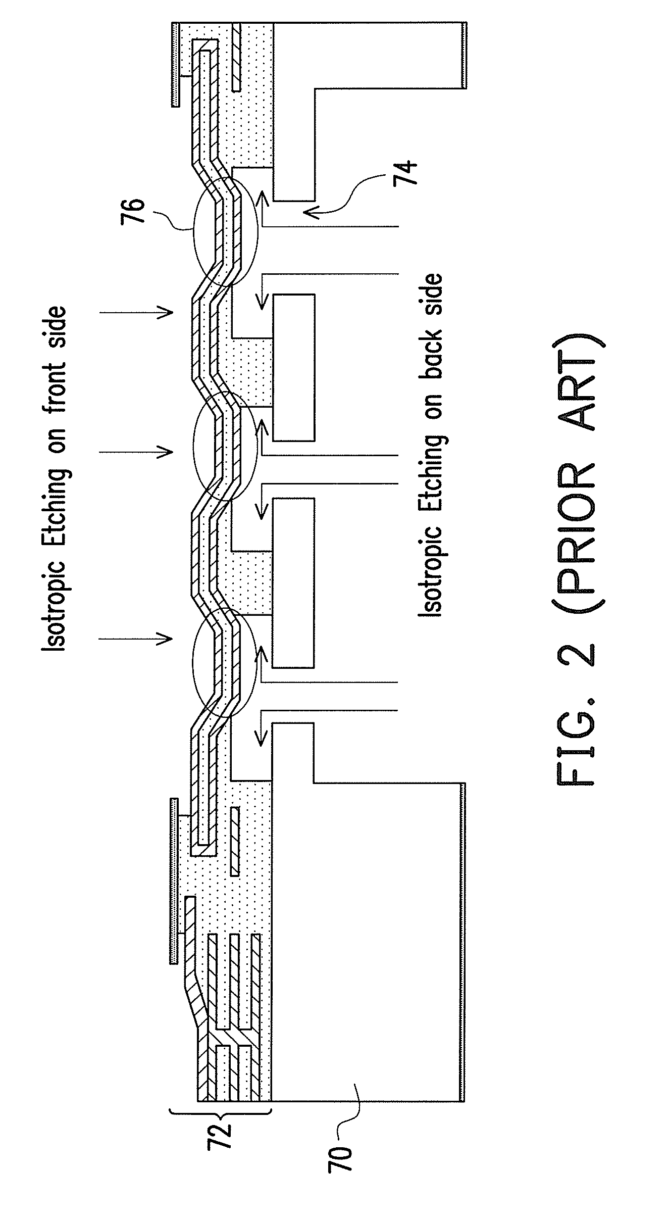
However, the dielectric material under the diaphragm is not etched fast because the etchant can only pass the venting holes 74 to etch the dielectric material and it usually takes a long etching time.
Therefore, when the dielectric layer in the gap is removed, the exposed portions 76 of the diaphragm may be damaged due to the long exposure on etchant solution.

Method used


Image

  • CMOS microelectromechanical system (MEMS) device and fabrication method thereof
  • CMOS microelectromechanical system (MEMS) device and fabrication method thereof
  • CMOS microelectromechanical system (MEMS) device and fabrication method thereof

Examples


Embodiment Construction

[0037]Several embodiments are provided for describing the invention but not for limiting the invention. Further, the embodiments can be properly combined to each other without limited to individual embodiments.

[0038]FIG. 3 is a cross-sectional view, schematically illustrating a MEMS device, according to an embodiment of the invention. In FIG. 3, the CMOS MEMS device includes the CMOS circuit90 and MEMS device 80, which are fabricated over the same substrate 100. The CMOS circuit 90 is fabricated by usual semiconductor fabricating process to form the circuit 120 with the bonding pad 122, for example. The circuit 120 is embedded in the dielectric layer 108, and is also referred as the structural dielectric layer 108 in the invention. The circuit 120 is a part the whole CMOS circuit, in which just the interconnection is shown. The structural dielectric layer 108 includes some device structure or interconnecting having been embedded in the dielectric. The MEMS device 80 includes a diaph...


PUM


Abstract

A method for fabricating the MEMS device includes providing a substrate. Then, a structural dielectric layer is formed over the substrate at a first side, wherein a diaphragm is embedded in the structural dielectric layer. The substrate is patterned from a second side to form a cavity in corresponding to the diaphragm and a plurality of venting holes in the substrate. An isotropic etching process is performed from the first side and the second side of the substrate via vent holes to remove a dielectric portion of the structural dielectric layer for exposing a central portion of the diaphragm while an end portion is held by a residue portion of the structural dielectric layer.

Description

BACKGROUND OF THE INVENTION[0001]1. Field of Invention[0002]The present invention relates to CMOS microelectromechanical system (MEMS) device and the fabrication method. More particularly, the present invention relates to CMOS microelectromechanical system (MEMS) device with reduced damaged during etching process.[0003]2. Description of Related Art[0004]The CMOS MEMS device usually includes the CMOS circuit and the MEMS device, which are fabricated at the same substrate by semiconductor fabrication process. For the MEMS device with a sensing diaphragm, such as the microphone diaphragm or other application, a long etching process may be included for etching most of material including dielectric and silicon substrate. Since the device is under a long time of etching process, the MEMS structure may be damaged.[0005]FIG. 1 is a cross-sectional view, schematically illustrating a conventional MEMS device at the stage to etch the substrate. As the issues noted by the present invention, in ...

Claims


Application Information

Patent Timeline
Patent Type & Authority Patents(United States)
IPC IPC(8): H01L21/8238
CPCB81C1/00246G01P15/0802G01P15/125G01L9/0042B81B2201/0235B81C2203/0714G01P2015/0828
Inventor HSIEH, TSUNG-MINLEE, CHIEN-HSING
Owner SOLID STATE SYST
Learn More