Methods to shape the electric field in electron devices, passivate dislocations and point defects, and enhance the luminescence efficiency of optical devices

a technology of electron devices and fluorine treatment, applied in the direction of semiconductor devices, basic electric elements, electrical equipment, etc., can solve the problems of increased leakage current, reduced breakdown voltage, and not suited to high-power applications, so as to increase the output power of the semiconductor device, reduce the leakage current of the gate, and increase the breakdown voltage

Active Publication Date: 2012-02-14
RGT UNIV OF CALIFORNIA
View PDF15 Cites 47 Cited by
  • Summary
  • Abstract
  • Description
  • Claims
  • Application Information

AI Technical Summary

Benefits of technology

[0029]The fluorine treatment may shape the electric field's profile or distribution in the electron device in 1, 2, or 3 dimensions. The electric field's shaping may allow a reduction in a peak electric field in a channel of an electron device, which increases breakdown voltage and decreases gate leakage without harming the electron device's high-frequency performance.
[0043]The present invention envisages a wide range of devices fabricated using this method, for example HEMTs, FETs, or nitride based devices. The amount of controlled dispersion is a trade off between reducing the peak electric field and minimizing a degradation of RF performance.

Problems solved by technology

Unfortunately, this method is not suited for high power applications, as the output power that results from this trade-off of current versus voltage is roughly constant.
In GaAs devices, the gate leakage has been identified as the main cause for the reduction of the breakdown voltage.
At that point the transistor enters in breakdown regime and impact ionization of the carriers occurs, leading to increased leakage current and ultimately to the destruction of the device.
However, the recess engineering method presents several important problems.
First, it introduces parasitic resistances that will harm the frequency performance of the device.
In particular, the method increases the drain access resistance, which in turn decreases the high frequency performance of the device.
This wet etch is not available for many semiconductor families, such as the nitrides for example.
Third, the use of recesses in the access region decreases the distance between the channel and the surface of the semiconductor.
This is likely to introduce dispersion in nitride-based devices, due to the higher effect of surface traps when they are close to the channel.
Finally, another problem of multiple recesses is that the dry etch induces damage into the semiconductor that significantly increases the gate leakage of the devices.
However, this second approach has the problem of significantly increasing the parasitic capacitances of the device. FIG. 3 shows how, in a transistor, as the thickness of the silicon nitride layer is increased, and when the FP is added to transistor, there is a parasitic increase in the gate-drain capacitance Cgd.
Therefore, this method is not a good option for high frequency devices [5,6], for example, high power devices operating at frequencies higher than 20 GHz.
Although a transistor was used as an example, the parasitic increase in capacitance is also present in other similar devices.

Method used


Image

  • Methods to shape the electric field in electron devices, passivate dislocations and point defects, and enhance the luminescence efficiency of optical devices
  • Methods to shape the electric field in electron devices, passivate dislocations and point defects, and enhance the luminescence efficiency of optical devices
  • Methods to shape the electric field in electron devices, passivate dislocations and point defects, and enhance the luminescence efficiency of optical devices

Examples


Embodiment Construction

[0060]In the following description of the preferred embodiment, reference is made to the accompanying drawings which form a part hereof, and in which is shown by way of illustration a specific embodiment in which the invention may be practiced. It is to be understood that other embodiments may be utilized and structural changes may be made without departing from the scope of the present invention.

[0061]Overview

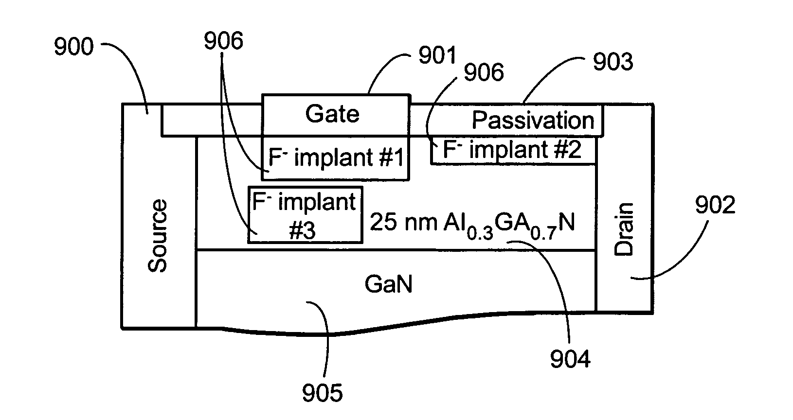
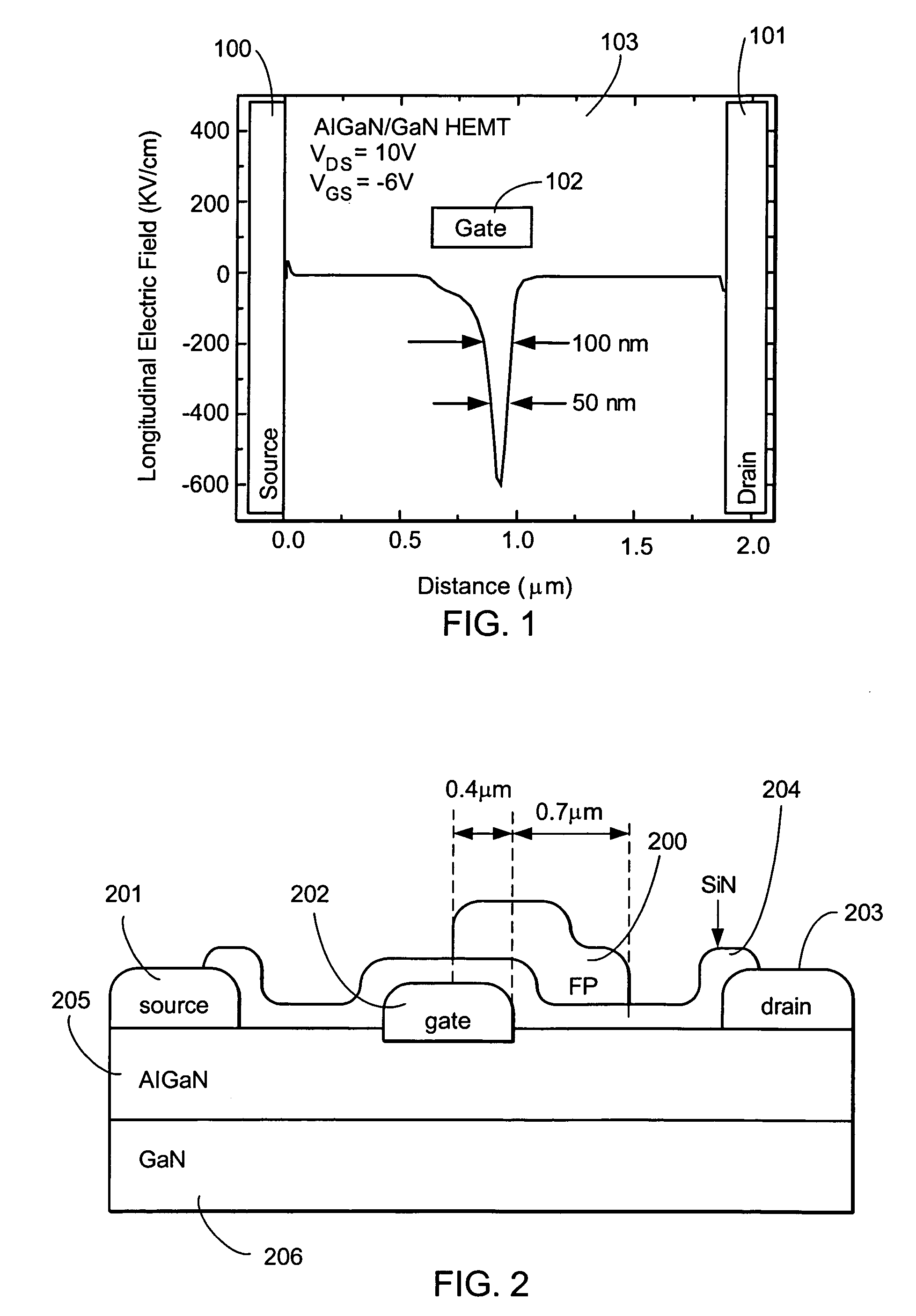
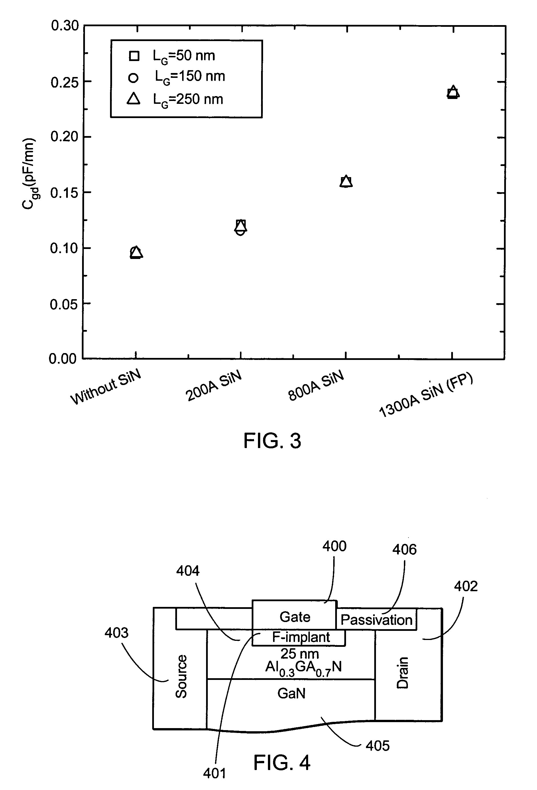
[0062]Treatments with fluorine compounds, including exposure to a plasma comprising fluorine containing compounds, have been used to locally reduce the electron concentration in nitride-based semiconductors, and shape the electric field profile in electron devices. The use of this electric field shaping technology, which can be employed in 1, 2, or 3-dimensional manner, in AlGaN / GaN HEMTs, allows a reduction in the peak electric field in the channel, which increases the breakdown voltage and decreases the gate leakage in these devices, without harming the high frequency perfor...


PUM


Abstract

A fluorine treatment that can shape the electric field profile in electronic devices in 1, 2, or 3 dimensions is disclosed. A method to increase the breakdown voltage of AlGaN / GaN high electron mobility transistors, by the introduction of a controlled amount of dispersion into the device, is also disclosed. This dispersion is large enough to reduce the peak electric field in the channel, but low enough in order not to cause a significant decrease in the output power of the device. In this design, the whole transistor is passivated against dispersion with the exception of a small region 50 to 100 nm wide right next to the drain side of the gate. In that region, surface traps cause limited amounts of dispersion, that will spread the high electric field under the gate edge, therefore increasing the breakdown voltage. Three different methods to introduce dispersion in the 50 nm closest to the gate are described: (1) introduction of a small gap between the passivation and the gate metal, (2) gradually reducing the thickness of the passivation, and (3) gradually reducing the thickness of the AlGaN cap layer in the region close the gate.

Description

CROSS-REFERENCE TO RELATED APPLICATIONS[0001]This application claims the benefit under 35 U.S.C Section 119(e) of U.S. Provisional Application Ser. No. 60 / 736,628, filed on Nov. 15, 2005, by Tomas Palacios, Likun Shen and Umesh K. Mishra, entitled “FLUORINE TREATMENT TO SHAPE THE ELECTRIC FIELD IN ELECTRON DEVICES, PASSIVATE DISLOCATIONS AND POINT DEFECTS, AND ENHANCE THE LUMINESCENCE EFFICIENCY OF OPTICAL DEVICES,” (2006-129);[0002]Which application is incorporated by reference herein.[0003]This application is related to the following co-pending and commonly-assigned application:[0004]U.S. Utility application Ser. No. 10 / 570,964, filed on Mar. 8, 2006, by Alessandro Chini, Umesh K. Mishra, Primit Parikh and Yifeng Wu, entitled “FABRICATION OF SINGLE OR MULTIPLE GATE FIELD PLATES”, now U.S. Pat. No. 7,812,369, issued Oct. 12, 2010, (2004-091), which application claims the benefit under 35 U.S.C Section 365(c) of PCT Application Serial No. US2004 / 029324, filed on Sep. 9, 2004, by Ale...

Claims


Application Information

Patent Timeline
Patent Type & Authority Patents(United States)
IPC IPC(8): H01L21/335
CPCH01L29/2003H01L29/207H01L29/402H01L29/66462H01L29/7786H01L29/7787H01L33/0095
Inventor PALACIOS, TOMASSHEN, LIKUNMISHRA, UMESH K.
Owner RGT UNIV OF CALIFORNIA
Why Eureka
Try Eureka