Display device and method for manufacturing the same

a technology for display devices and manufacturing methods, applied in semiconductor devices, instruments, optics, etc., can solve problems such as the reduction of aperture ratios, and achieve the effects of reducing manufacturing costs, convenient breakage, and excellent electric characteristics

Active Publication Date: 2012-02-14
SEMICON ENERGY LAB CO LTD
View PDF137 Cites 42 Cited by
  • Summary
  • Abstract
  • Description
  • Claims
  • Application Information

AI Technical Summary

Benefits of technology

[0010]In particular, as the pixel density of the display device is increased, writing time of a display image is reduced. Therefore, it is preferable that the transistor used for the driver circuit operate at high speed. Besides, the increased pixel density causes a decrease in the aperture ratio, which is a problem in the pixel portion.
[0031]With use of an oxide semiconductor layer subjected to heat treatment for dehydration or dehydrogenation, a transistor with excellent electric characteristics can be manufactured. Further, when the transistor for the pixel circuit is formed using a light-transmitting material, a display device having high aperture ratio and excellent display characteristics can be manufactured. Furthermore, in a display device in which the pixel circuit and a driver circuit are formed over one substrate, transistors included in the pixel circuit and the driver circuit can be formed to have different structures between the circuits in order to obtain electric characteristics needed for the respective circuits easily.

Problems solved by technology

Besides, the increased pixel density causes a decrease in the aperture ratio, which is a problem in the pixel portion.

Method used


Image

  • Display device and method for manufacturing the same
  • Display device and method for manufacturing the same
  • Display device and method for manufacturing the same

Examples


embodiment 1

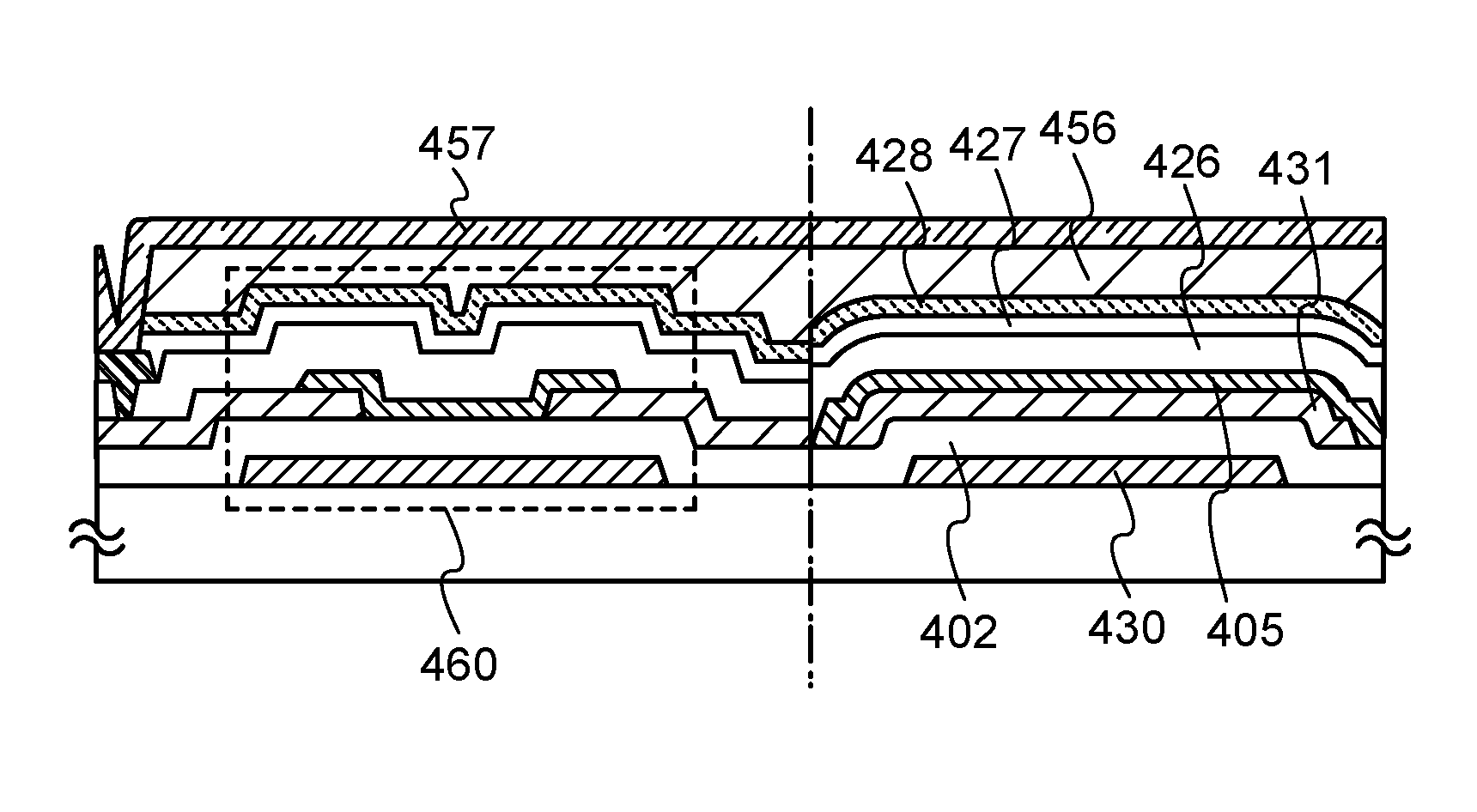
[0061]In this embodiment, a display device and a manufacturing method thereof will be described in detail with reference to drawings. FIG. 1E illustrates an example of a cross-sectional structure of a transistor in a driver circuit, a transistor in a pixel portion, and a contact portion of a gate wiring (gate electrode), which are formed over one substrate.

[0062]A transistor 450 has a bottom-gate structure called a channel-etch type, and a transistor 460 has a bottom-gate structure called a bottom-contact (also called an inverted-coplanar) type.

[0063]The transistor 460 provided in the pixel includes, over a substrate 400 having an insulating surface, a gate electrode layer 451a, a gate insulating layer 402, an oxide semiconductor layer 454 including a channel formation region, a source electrode layer 455a, and a drain electrode layer 455b. In addition, an oxide insulating layer 426 which covers the transistor 460 and is in contact with an upper surface and a side surface of the oxi...

embodiment 2

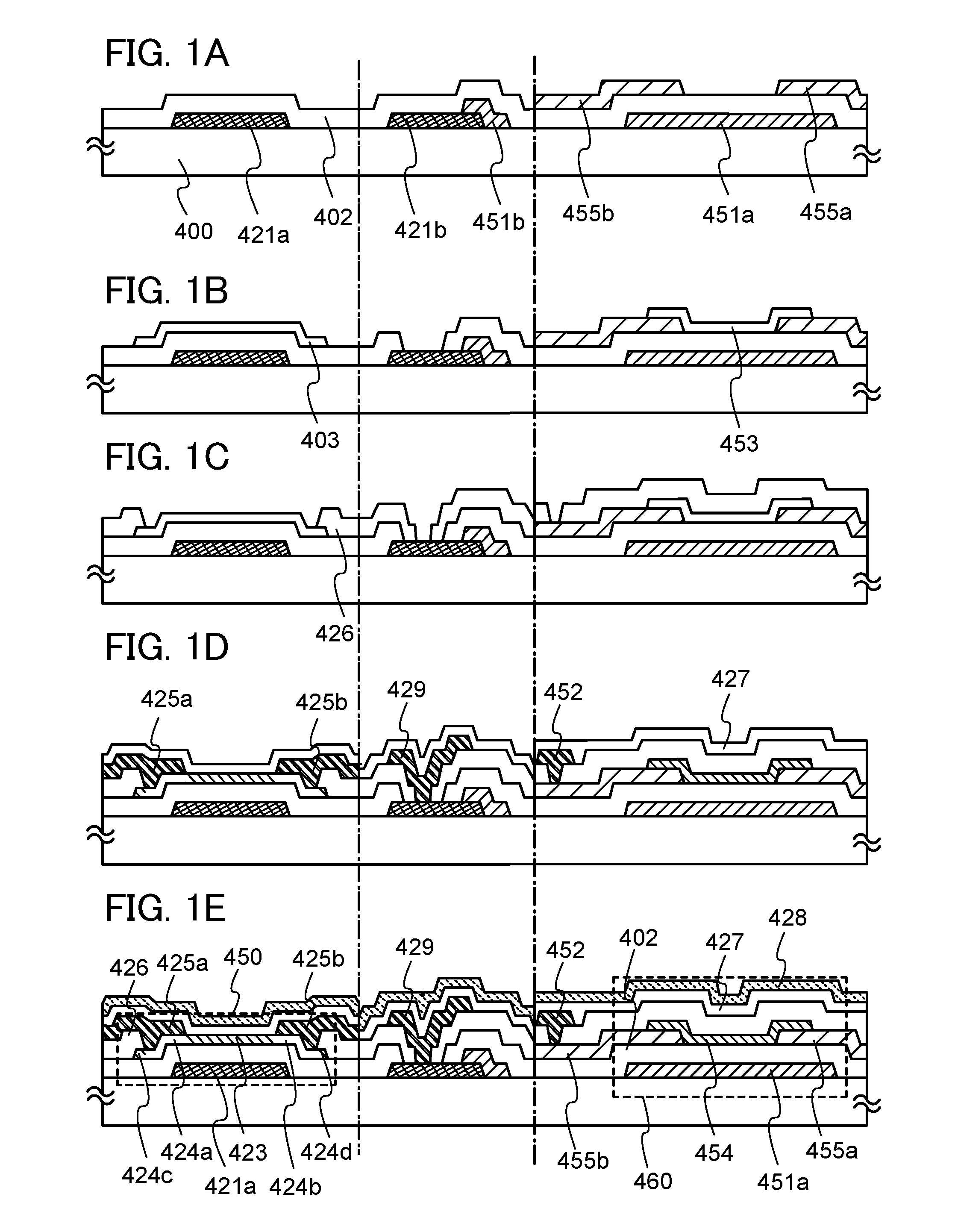
[0126]In this embodiment, an example of a transistor whose manufacturing process is partly different from that of Embodiment 1 will be described with reference to FIGS. 2A to 2E. FIGS. 2A to 2E are the same as FIGS. 1A to 1E except that there is a difference in part of the process. Therefore, the same portions are denoted by the same reference numerals, and detailed description of the same portions is omitted.

[0127]First, in accordance with Embodiment 1, the gate electrode layers 421a and 451a and the gate insulating layer 402 are formed over the substrate, and then the source electrode layer 455a and the drain electrode layer 455b are formed to partly overlap with the gate electrode layer 451a with the gate insulating layer 402 interposed therebetween. Then, an oxide semiconductor film is formed over the gate insulating layer 402, the source electrode layer 455a, and the drain electrode layer 455b.

[0128]Then, the oxide semiconductor film is subjected to dehydration or dehydrogenat...

embodiment 3

[0153]In this embodiment, an example in which a liquid crystal display device is manufactured with the active-matrix substrate described in Embodiment 1 or 2 will be described.

[0154]FIG. 3 illustrates an example of a cross-sectional structure of an active-matrix substrate.

[0155]Embodiments 1 and 2 show the example in which the transistor for the driver circuit portion, the transistor for the pixel portion, and the gate wiring (gate electrode) contact portion are formed over one substrate. In this embodiment, in addition to the above components, a storage capacitor and an intersection of the gate wiring and the source wiring are illustrated and described.

[0156]The capacitor, the gate wiring, and the source wiring can be formed in the same manufacturing steps as those in Embodiment 1 or 2, without an increase in the number of photomasks and an increase in the number of steps. Further, in a portion serving as a display region in a pixel portion, the gate wiring, the source wiring, and ...


PUM

PropertyMeasurementUnit
temperatureaaaaaaaaaa
gate threshold voltageaaaaaaaaaa

Abstract

An object is to provide a display device with excellent display characteristics, where a pixel circuit and a driver circuit provided over one substrate are formed using transistors which have different structures corresponding to characteristics of the respective circuits. The driver circuit portion includes a driver circuit transistor in which a gate electrode layer, a source electrode layer, and a drain electrode layer are formed using a metal film, and a channel layer is formed using an oxide semiconductor. The pixel portion includes a pixel transistor in which a gate electrode layer, a source electrode layer, and a drain electrode layer are formed using an oxide conductor, and a semiconductor layer is formed using an oxide semiconductor. The pixel transistor is formed using a light-transmitting material, and thus, a display device with higher aperture ratio can be manufactured.

Description

BACKGROUND OF THE INVENTION[0001]1. Field of the Invention[0002]The present invention relates to a display device including an oxide semiconductor.[0003]2. Description of the Related Art[0004]In recent years, a technique by which transistors are formed using semiconductor thin films formed over a substrate having an insulating surface has been attracting attention. The transistors are applied to a wide range of electronic devices such as ICs or electro-optical devices, and there is an expectation for immediate development of especially transistors to be used as switching elements for image display devices. Various metal oxides are used for a variety of applications. Indium oxide is a well-known material and is used as a transparent electrode material which is necessary for liquid crystal displays and the like.[0005]Some metal oxides have semiconductor characteristics. Examples of such metal oxides having semiconductor characteristics include tungsten oxide, tin oxide, indium oxide, ...

Claims


Application Information

Patent Timeline
Patent Type & Authority Patents(United States)
IPC IPC(8): G02F1/136
CPCH01L27/1225H01L27/1251H01L29/66969H01L27/1259H01L21/02664H01L21/477H01L21/02565H01L21/324H01L21/77H01L27/12H01L29/45H01L29/4908G02F1/133345G02F1/1368H01L27/1248H01L29/7869H01L29/78696
Inventor YAMAZAKI, SHUNPEISAKATA, JUNICHIROTSUBUKU, MASASHIAKIMOTO, KENGOHOSOBA, MIYUKISAKAKURA, MASAYUKIOIKAWA, YOSHIAKI
Owner SEMICON ENERGY LAB CO LTD
Why Eureka
Try Eureka