

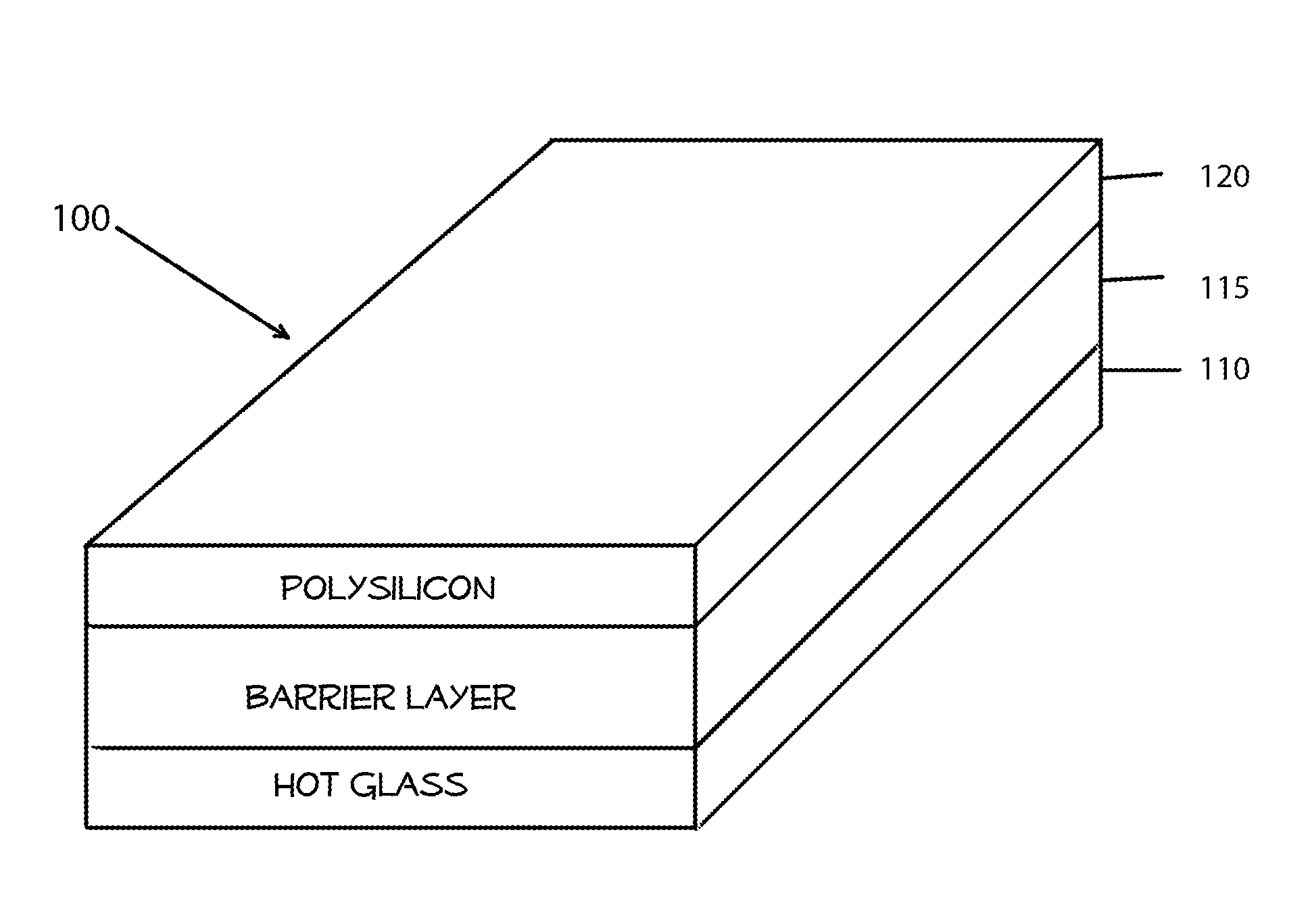
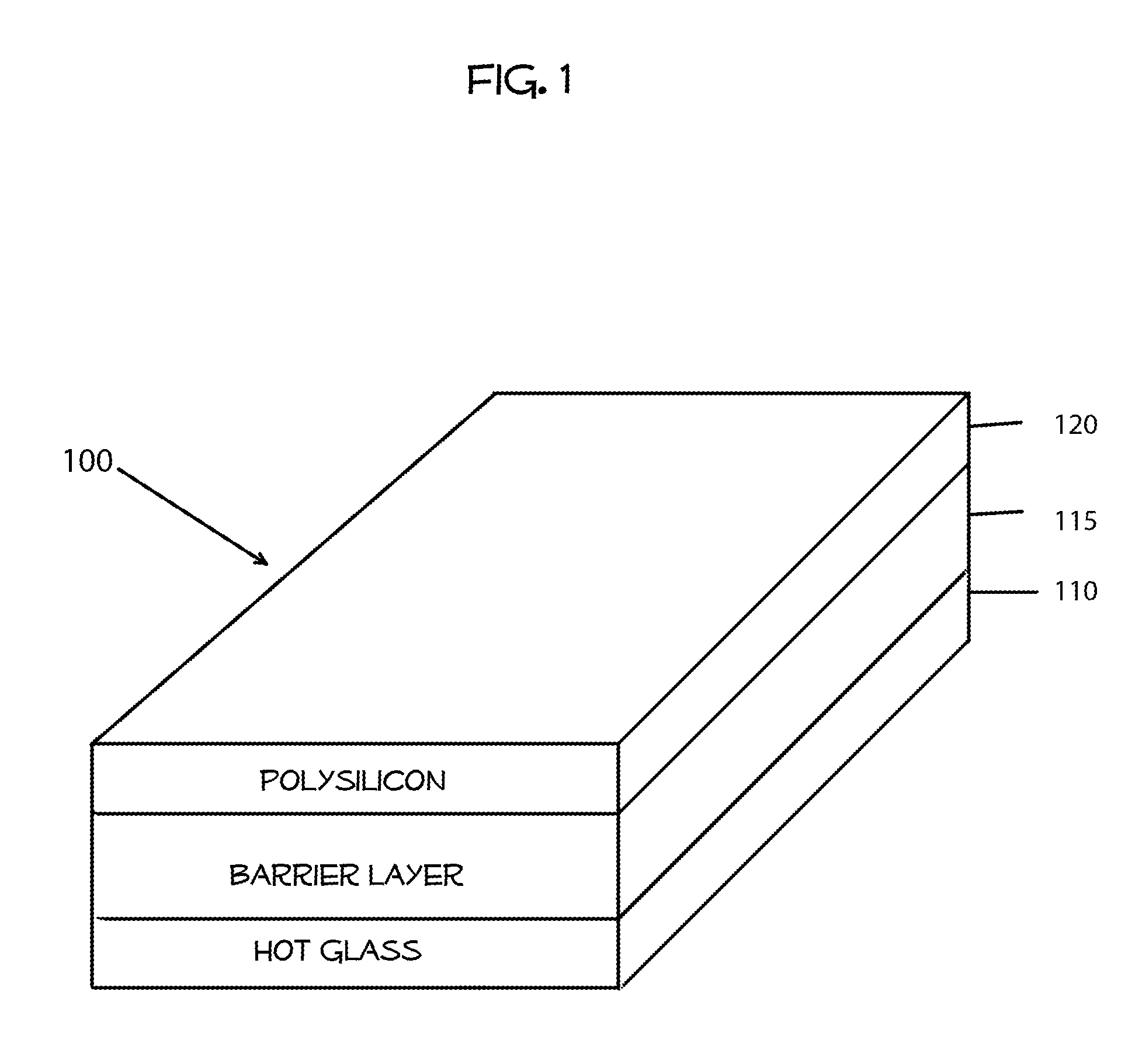
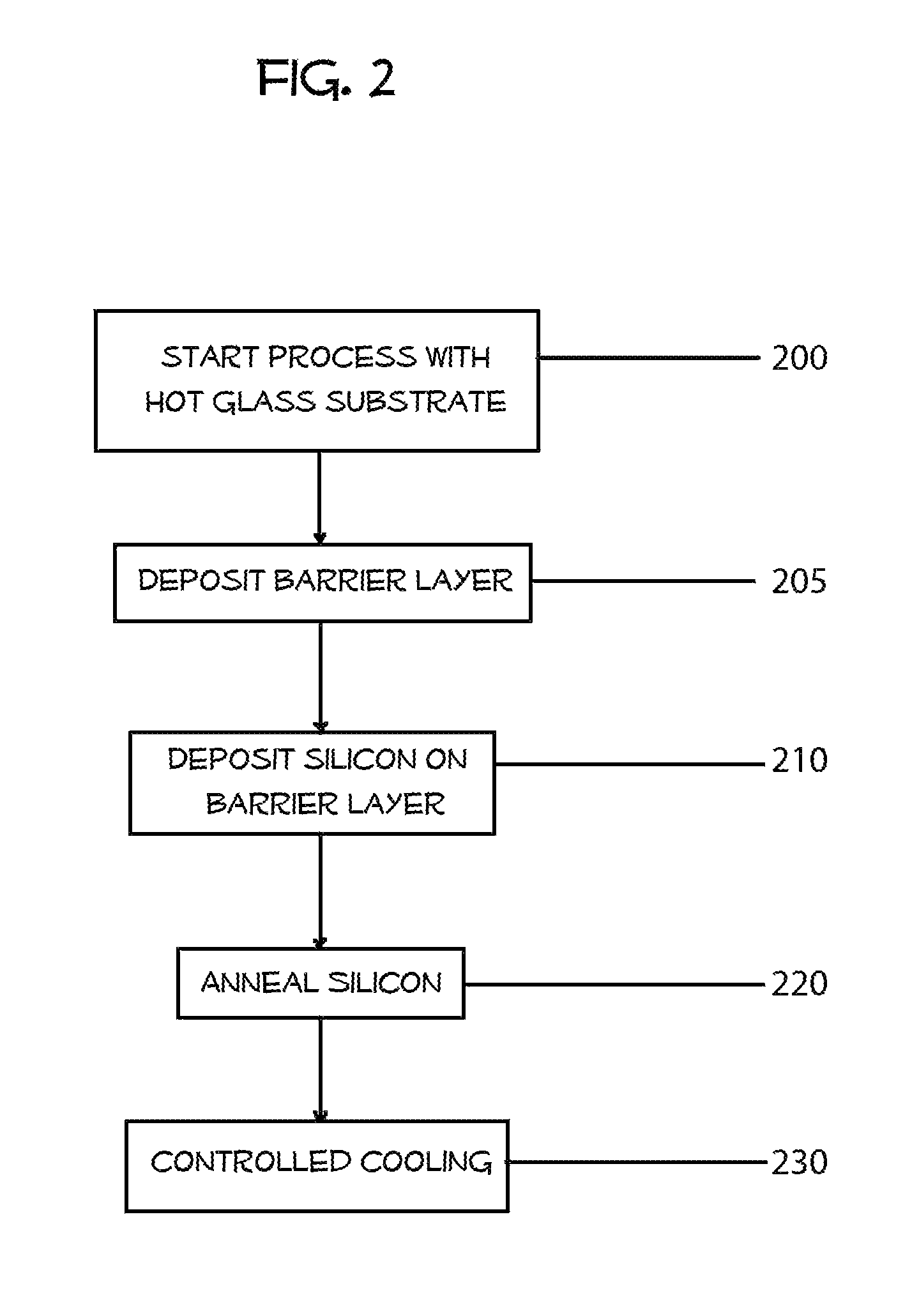
Method for producing high temperature thin film silicon layer on glass
a technology of high temperature thin film and glass, which is applied in the direction of coatings, solid-state devices, chemical vapor deposition coatings, etc., can solve the problems of reduced efficiency, amorphous silicon transistors introducing other significant limitations, and high temperature processes are not suitable for substrates made of plastics or other materials, so as to achieve faster transistor speed and faster production cycle time , the effect of large grain size ratio
- Summary
- Abstract
- Description
- Claims
- Application Information
AI Technical Summary
Benefits of technology
Problems solved by technology
Method used
Image

Examples
Embodiment Construction
[0040]All numbers expressing dimensions, physical characteristics, quantities of ingredients, reaction conditions, and the like used in the specification and claims are to be understood as being modified in all instances by the term “about”. Accordingly, unless indicated to the contrary, the numerical values set forth in the following specification and claims may vary depending upon the desired properties sought to be obtained by the present invention. At the very least, and not as an attempt to limit the application of the doctrine of equivalents to the scope of the claims, each numerical parameter should at least be construed in light of the number of reported significant digits and by applying ordinary rounding techniques. Moreover, all ranges disclosed herein are to be understood to encompass any and all sub-ranges subsumed therein. For example, a stated range of “1 to 10” should be considered to include any and all sub-ranges between (and inclusive of) the minimum value of 1 an...
PUM
| Property | Measurement | Unit |
|---|---|---|
| Temperature | aaaaa | aaaaa |
| Temperature | aaaaa | aaaaa |
| Resolution enthalpy | aaaaa | aaaaa |
Abstract
Description
Claims
Application Information