Semiconductor element and manufacturing method therefor

a technology of semiconductor elements and semiconductors, applied in the field of semiconductor devices, can solve the problems of reducing the contact resistance of the mosfet, affecting the operation of the parasitic bipolar transistor inside the vertical mosfet, and reducing the contact resistance. the effect of reducing the delay of switching, reducing the deterioration of performance due to misalignment, and reducing the contact resistan

Active Publication Date: 2012-03-06
PANASONIC CORP
View PDF20 Cites 0 Cited by
  • Summary
  • Abstract
  • Description
  • Claims
  • Application Information

AI Technical Summary

Benefits of technology

[0064]In a semiconductor device according to the present invention, including n- and p-type semiconductor regions on the surface of a semiconductor layer and a conductor with a conductive surface that contacts with those semiconductor regions, even if the conductive surface is misaligned with the semiconductor regions, the deterioration in performance due to the misalignment can be minimized. As a result, the present invention always ensures device performance at an acceptable level.
[0065]Particularly when the present invention is applied to a vertical MOSFET, even if a source electrode being formed on a semiconductor layer by photolithographic process is misaligned with a contact region that has been defined on the surface of the semiconductor layer, a sufficient area of contact can still be ensured between the source electrode and the contact region and their contact resistance can be kept low. Consequently, switching delay that could be caused by the operation of a parasitic bipolar transistor inside a vertical MOSFET can be minimized. On top of that, even if the degree of misalignment has increased, the variation in the length Z of the periphery of the conductive surface that crosses the contact region can be reduced to a low level. As a result, a sufficient effective gate width, and therefore, a sufficient amount of ON-state current, can be ensured just as designed. In addition, the variation in ON-state resistance between products can also be reduced so much as to increase the yield significantly.
[0066]Furthermore, according to the present invention, such a semiconductor device can be fabricated without complicating the manufacturing process.

Problems solved by technology

An electric circuit with such a coil, however, will produce induced current during switching.
Then, part of the induced current would flow instantaneously around the channel layer 106, thus possibly damaging the channel or gate portion of the MOSFET.
That induced current could also delay switching of the MOSFET.
Generally speaking, however, a size shift or a misalignment could occur in a photolithographic process.
As long as a known exposure system is used, it is very difficult to avoid the misalignment perfectly.
Specifically, even if a stepper is used, a misalignment of 0.5 μm or more could be caused.

Method used


Image

  • Semiconductor element and manufacturing method therefor
  • Semiconductor element and manufacturing method therefor
  • Semiconductor element and manufacturing method therefor

Examples


embodiment 1

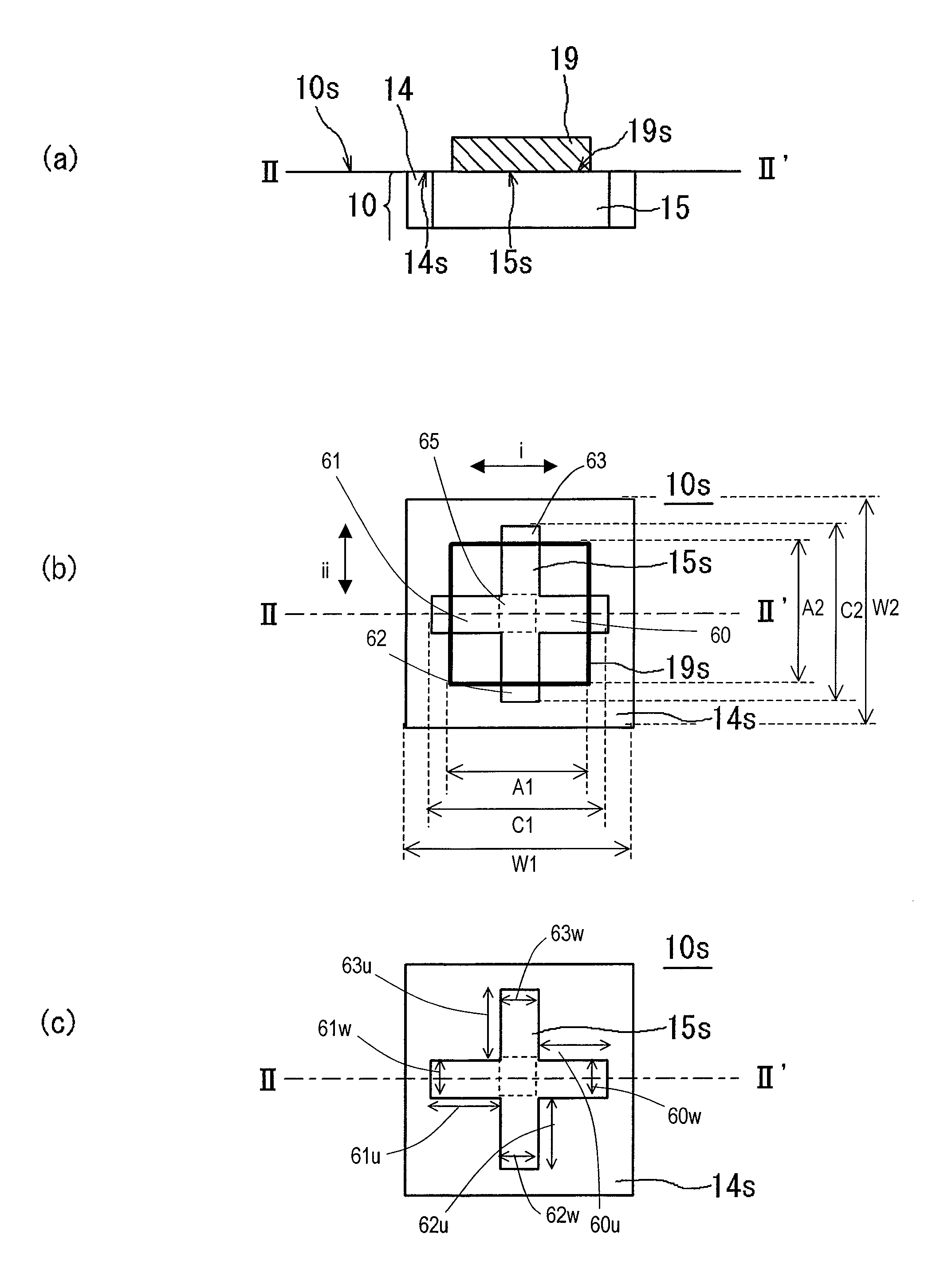
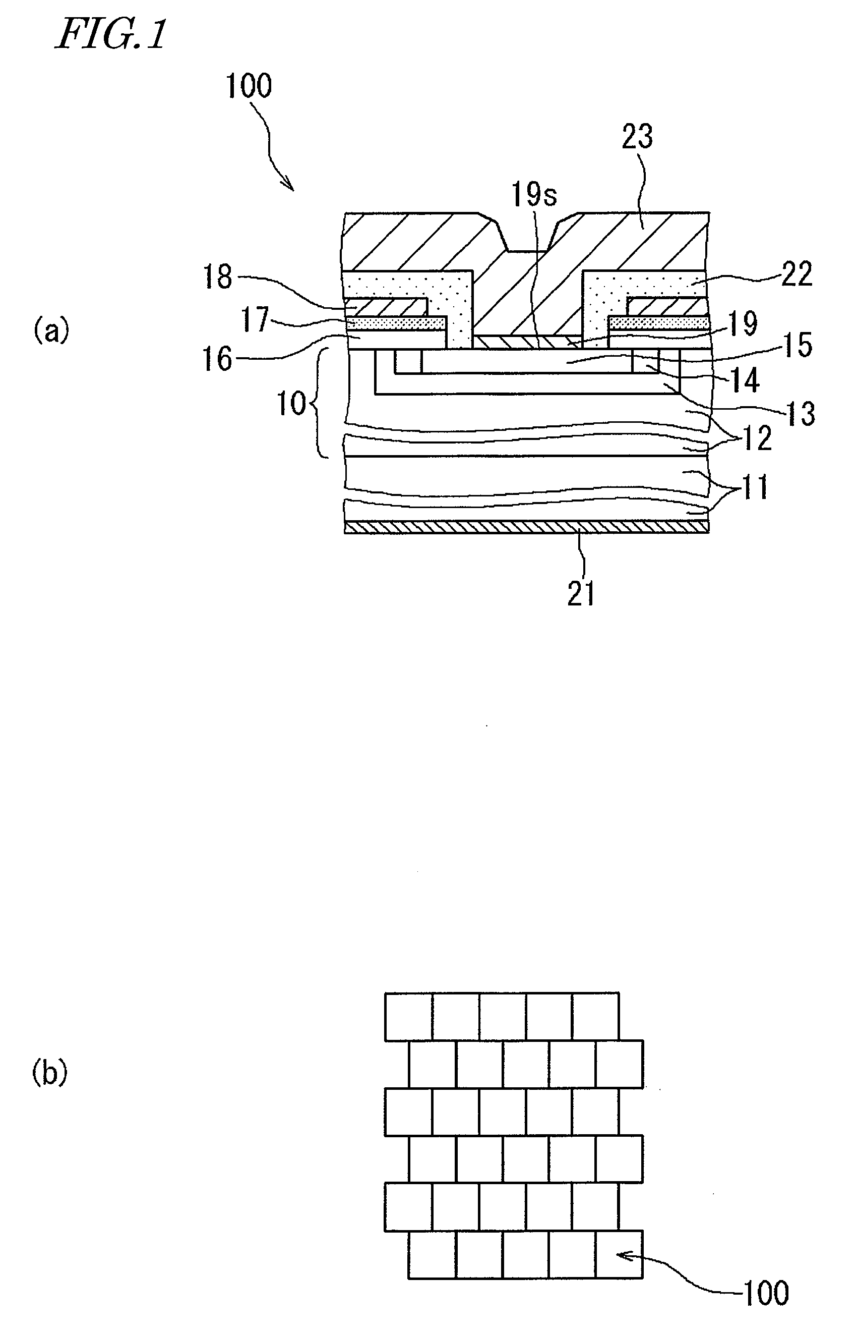
[0120]Hereinafter, a first specific preferred embodiment of a semiconductor device according to the present invention will be described with reference to FIGS. 1 through 4. The semiconductor device of this preferred embodiment is a vertical MOSFET that uses silicon carbide.

[0121]The semiconductor device of this preferred embodiment includes at least one unit cell including a semiconductor layer, source and drain electrodes that are electrically connected to the semiconductor layer, and a gate electrode for use to switch the semiconductor device between ON and OFF states, and typically has a structure in which a number of such unit cells are arranged. In the following description, a semiconductor device consisting of a plurality of unit cells with a substantially quadrangular planar shape will be taken as an example.

[0122]FIGS. 1(a) and 1(b) are respectively a schematic cross-sectional view illustrating a unit cell of this preferred embodiment and a plan view illustrating an arrangem...

embodiment 2

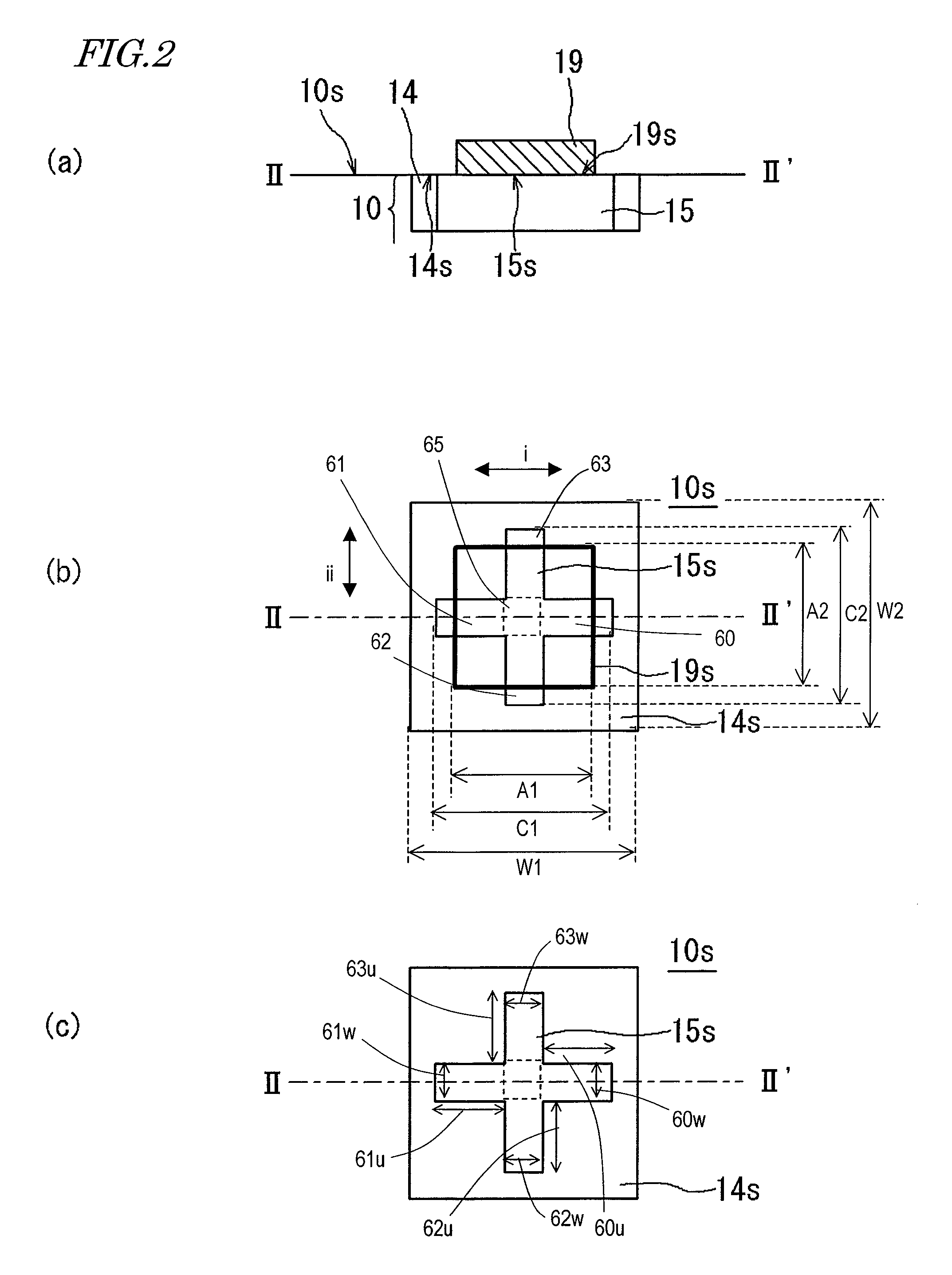
[0198]Hereinafter, a second preferred embodiment of a semiconductor device according to the present invention will be described with reference to the accompanying drawings. The semiconductor device of this preferred embodiment is also a vertical MOSFET but is different from its counterpart of any of the preferred embodiments described above in that the source region has a polygonal surface shape on the surface of the semiconductor layer and that the respective strip portions of the contact region extend toward the vertices of the polygonal source region.

[0199]The present inventors also discovered via experiments that in the conventional semiconductor device shown in FIG. 41, as the degree of misalignment increased, not just the area of contact between the contact region and the conductive surface of the source electrode decreased but also an another problem would arise as will be described below. Such an additional problem will be described with reference to FIGS. 43(a) and 43(b).

[0...

embodiment 3

[0269]Hereinafter, a third preferred embodiment of a semiconductor device according to the present invention will be described with reference to the accompanying drawings. The semiconductor device of this preferred embodiment is a vertical MOSFET that uses silicon carbide but consists of striped unit cells unlike the counterparts of the preferred embodiments described above. In the following description, a comb shaped MOSFET, unit cells of which have stripes that run perpendicularly to the direction in which electrons flow through the channel, will be described as an example.

[0270]FIG. 36(a) is a schematic cross-sectional view illustrating an exemplary unit cell as a third preferred embodiment of the present invention. FIG. 36(b) is a top view illustrating the arrangement of the unit cells in the semiconductor device of this preferred embodiment. For the sake of simplicity, any pair of components shown in both FIGS. 1(a) and 1(b) and FIGS. 36(a) and 36(b) and having substantially th...


PUM


Abstract

A semiconductor device includes: a semiconductor layer including silicon carbide, which has been formed on a substrate; a semiconductor region 15 of a first conductivity type defined on the surface of the semiconductor layer 10; a semiconductor region 14 of a second conductivity type, which is defined on the surface 10s of the semiconductor layer so as to surround the semiconductor region 15 of the first conductivity type; and a conductor 19 with a conductive surface 19s that contacts with the semiconductor regions 15 and 14 of the first and second conductivity types. On the surface 10s of the semiconductor layer, the semiconductor region 15 of the first conductivity type has at least one first strip portion 60 that runs along a first axis i. The width C1 of the semiconductor region 15 of the first conductivity type as measured along the first axis i is greater than the width A1 of the conductive surface 19s as measured along the first axis i. And the periphery of the conductive surface 19s crosses the at least one first strip portion 60, 61.

Description

TECHNICAL FIELD[0001]The present invention relates to a semiconductor device and a method for fabricating the same. More particularly, the present invention relates to a power semiconductor device of silicon carbide, which can be used in applications that require a high breakdown voltage and a large amount of current.BACKGROUND ART[0002]Silicon carbide (SiC) is a high-hardness semiconductor material with a greater bandgap than silicon (Si), and has been used extensively in various types of semiconductor devices including power elements, hostile-environment elements, high temperature operating elements, and radio frequency elements. Among other things, the application of SiC to power elements such as switching elements and rectifiers has attracted a lot of attention. This is because a power element that uses SiC can significantly reduce the power loss compared to a Si power element.[0003]Among various power elements that use SiC, a MOSFET is known as a typical switching element. Such...

Claims


Application Information

Patent Timeline
Patent Type & Authority Patents(United States)
IPC IPC(8): H01L27/10
CPCH01L29/0696H01L29/66068H01L29/7802H01L29/7828H01L29/1608
Inventor UCHIDA, MASAOHAYASHI, MASASHIHASHIMOTO, KOICHI
Owner PANASONIC CORP
Why Eureka
Try Eureka