AlGaInN-based lasers produced using etched facet technology

a laser and etched face technology, applied in the field of fabricating lasers, can solve the problems of incompatibility with monolithic integration, high price of these devices, and difficult cleaving of gan, so as to prevent damage to p-contact, enhance selectivity, and high selectivity

Active Publication Date: 2012-03-06
MACOM TECH SOLUTIONS HLDG INC
View PDF9 Cites 17 Cited by
  • Summary
  • Abstract
  • Description
  • Claims
  • Application Information

AI Technical Summary

Benefits of technology

[0005]A significant factor affecting the yield and cost of GaN-based blue lasers is the lack of availability of laser quality material with low defect density. A few research labs have developed techniques such as epitaxial lateral overgrowth (ELOG) on sapphire that have improved the defect density to the 105 / cm2 level. Because of the difficulty in cleaving, described previously, the minimum cavity length that can be realistically fabricated today is on the order of 600 μm. The use of etched facets in place of mechanically cleaved facets allows the formation of shorter cavity devices of 100 μm or less. The ability to make shorter cavity devices results in a lower probability of having defects in the device and hence produces a much higher yield. These lasers may have a lower maximum power rating than longer cavity devices; however, the vast majority of lasers will be used in next generation DVD read-only applications, where lower power is sufficient and the lowest cost and lowest power consumption will be needed. The specific fabrication, integration and full wafer testing capabilities enabled by EFT will also provide significant benefits to the fabrication of high-power GaN lasers for writable optical disk applications.SUMMARY OF THE INVENTION
[0006]In view of the attractiveness of an etched-facet blue-emitting laser from a process yield and cost perspective, as well as its potential for the fabrication of integrated AlGaInN-based photonics, a new EFT process has been developed to achieve facet etching in AlGaInN-based structures. Several years ago, a new technology was pioneered [A. Behfar-Rad, et al. 1989 Appl. Phys. Lett. 54, 439-495; U.S. Pat. No. 4,851,3682] in which laser facets were formed using a process based on photolithography definition of a mask and chemically assisted ion beam etching (CAIBE). BinOptics Corporation of Ithaca, N.Y., has developed commercially available InP-based laser products using this Etched Facet Technology (EFT). These products are characterized by precisely located mirrors that have a quality and reflectivity that are equivalent to those obtained by cleaving. With EFT, lasers are fabricated on the wafer in much the same way that integrated circuit chips are fabricated on silicon. This allows the lasers to be monolithically integrated with other photonic devices on a single chip and to be tested inexpensively at the wafer level [P. Vettiger, et al. 1991 IEEE J. Quantum Electron. 27, 1319-13314].
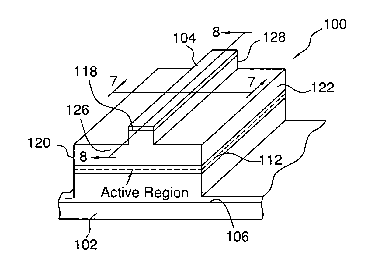
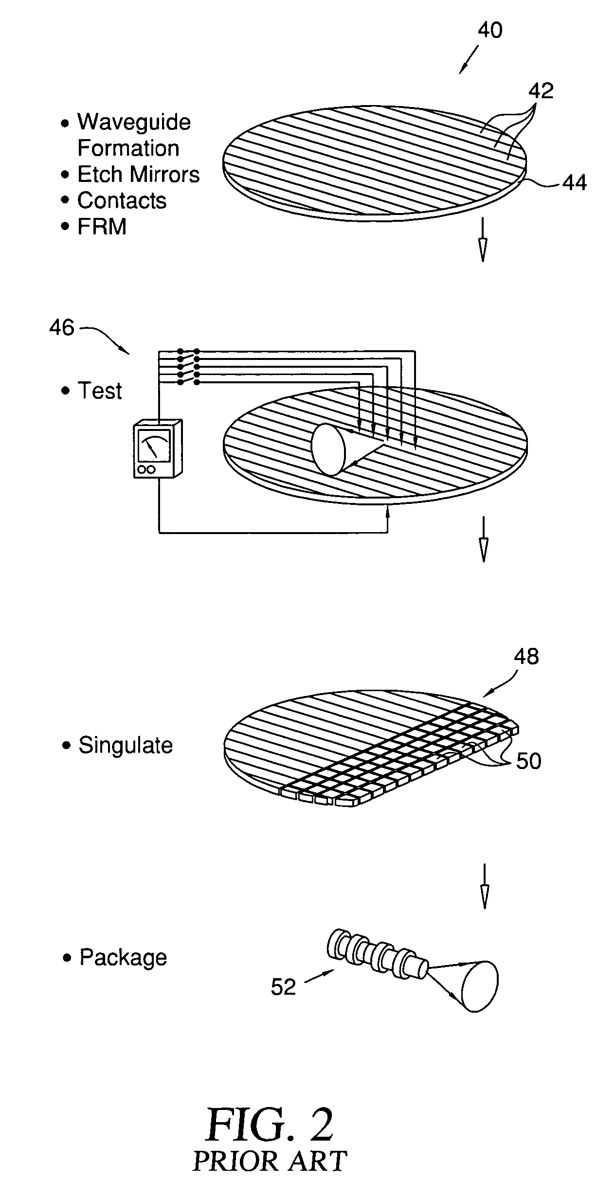
[0008]In accordance with the present invention, lasers are fabricated on a wafer in much the same way that integrated circuit chips are fabricated on silicon, so that the chips are formed in full-wafer form. The laser mirrors are etched on the wafer using the EFT process, and the electrical contacts for the lasers are fabricated. The lasers are tested on the wafer, and thereafter the wafer is singulated to separate the lasers for packaging. Scanning Electron Microscope images of etched AlGaInN-based facets show the degree of verticality and smoothness achieved using newly developed EFT process of the present invention. The present invention allows lasers and integrated devices for a variety of applications with wavelength requirements accessible with AlGaInN-based materials.
[0010]Selectivity between the etching of the semiconductor and the masking material is very important in obtaining straight surfaces for use in photonics. High selectivity between the mask and the GaN based substrate was obtained, in accordance with the present invention, by performing CAIBE at high temperatures. Large ion beam voltages in CAIBE were also found to enhance the selectivity. The mask materials were chosen to withstand the high temperature etching, but also to prevent damage to the p-contact of the GaN-based structure.

Problems solved by technology

It also tends to be incompatible with monolithic integration because it requires that the wafer be physically broken to obtain fully functional lasers.
Cleaving of GaN is especially problematic.
Cleaving is commonly used to form the facets of blue lasers, but the prices of these devices have remained very high.
Cleaving the sapphire substrate to form the GaN-based laser facets is particularly difficult, since-sapphire has many cleave planes with approximately equal cleave strength within a small angular distance of each other.
Because of this, the fracture interface can easily be redirected from one cleavage plane to another, even when perturbations during the cleaving process are small, and when this occurs, the laser is unusable.
However, both sapphire and the more expensive SiC substrates are significantly lattice mismatched to GaN, producing high defect densities in the grown material.
It is therefore expected that cleaving will continue to be a challenging process even with GaN substrates.
A significant factor affecting the yield and cost of GaN-based blue lasers is the lack of availability of laser quality material with low defect density.

Method used


Image

  • AlGaInN-based lasers produced using etched facet technology
  • AlGaInN-based lasers produced using etched facet technology
  • AlGaInN-based lasers produced using etched facet technology

Examples


Embodiment Construction

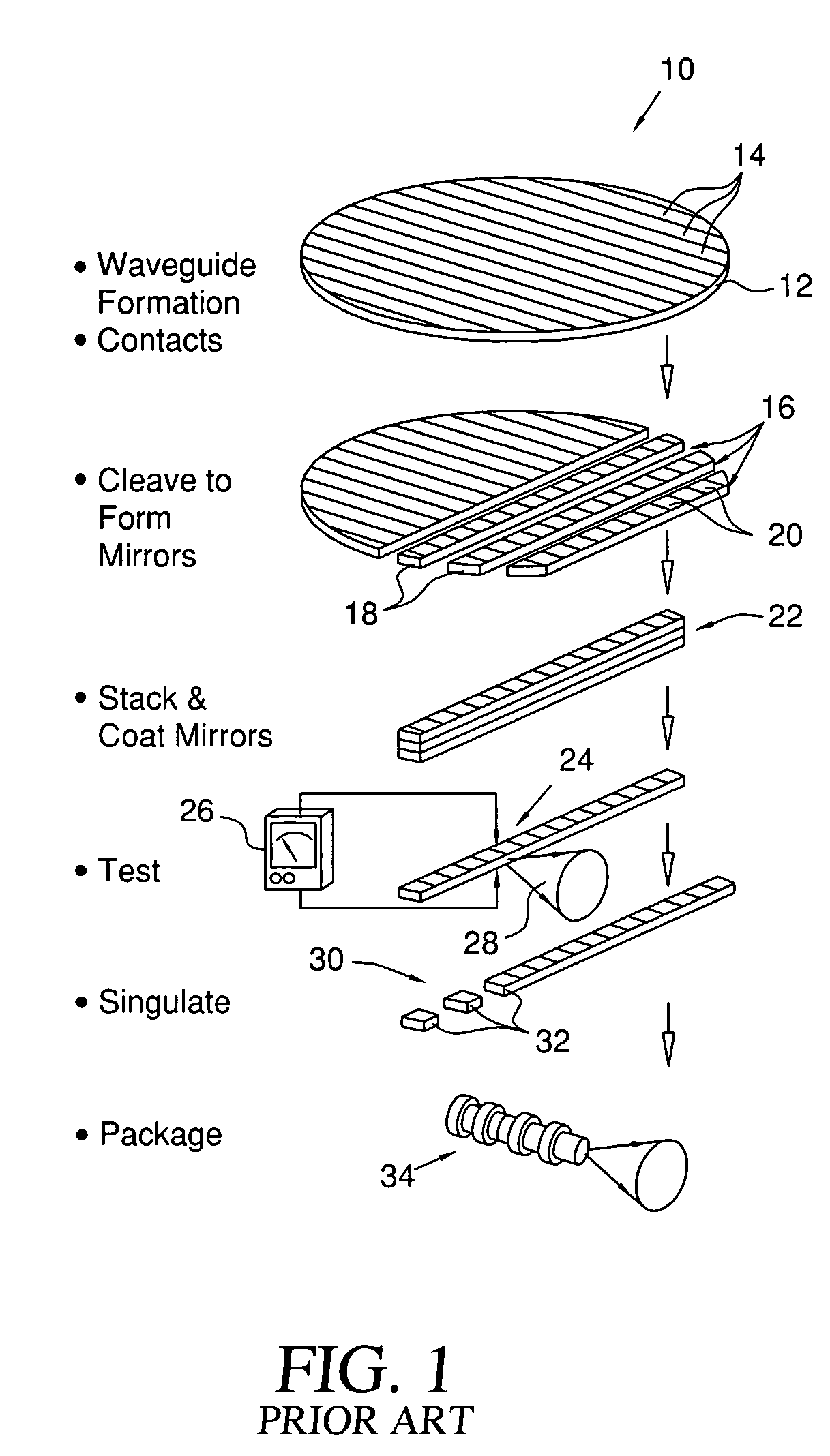
[0021]As generally illustrated at 10 in FIG. 1, mechanical cleaving of a semiconductor epi wafer 12 is the usual process for defining reflective mirrors, or facets, at the cavity ends of edge-emitting diode lasers. In this process, multiple waveguides 14 are fabricated on the wafer substrate, a metal contact layer is applied, and the wafer is mechanically cleaved, as along cleave lines 16, to form bars 18 of laser devices 20. The bars 18 are then stacked, as illustrated at 22, and the cleaved end facets of the laser devices are coated to provide the desired reflection and emission characteristics. The individual laser devices 20 may then be tested, as at 24, by applying a bias voltage 26 across the individual lasers, and detecting the resulting output light beam 28. The bars of laser devices may then be separated, or singulated, as at 30, to produce individual chips 32 that may be suitably packaged, in known manner, as at 34.

[0022]For most semiconductor devices, however, the foregoi...


PUM


Abstract

A process for fabricating lasers capable of emitting blue light wherein a GaN wafer is etched to form laser waveguides and mirrors using a temperature of over 500° C. and an ion beam in excess of 500 V in CAIBE.

Description

BACKGROUND OF THE INVENTION[0001]This application claims the benefit of U.S. Provisional Patent Application No. 60 / 692,583, filed Jun. 22, 2005, the disclosure of which is hereby incorporated herein by reference.[0002]The present invention relates, in general, to a process for fabricating lasers capable of emitting blue light, and, more particularly, to the fabrication of AlGaInN-based lasers utilizing etched facet technology (EFT) for producing laser devices.[0003]Reflective mirrors for edge-emitting semiconductor laser diodes are typically formed at the ends of a laser cavity by mechanical cleaving of a semiconductor crystal. In general, for any semiconductor material, cleaving is an imprecise process compared to photolithography. In addition, it necessitates the handling of fragile bars or miniscule chips for device testing and other subsequent operations. It also tends to be incompatible with monolithic integration because it requires that the wafer be physically broken to obtai...

Claims


Application Information

Patent Timeline
Patent Type & Authority Patents(United States)
IPC IPC(8): H01S5/00H01S5/185
CPCB82Y20/00H01S5/0201H01S5/0042H01S5/028H01S5/0203H01S5/0262H01S5/0264H01S5/1039H01S5/18H01S5/22H01S5/32341H01S5/34333H01S5/185
Inventor BEHFAR, ALEX A.SCHREMER, ALFRED T.STAGARESCU, CRISTIAN B.VAINATEYA
Owner MACOM TECH SOLUTIONS HLDG INC
Why Eureka
Try Eureka