Single-chamber sequential curing of semiconductor wafers

a technology of semiconductor wafers and curing chambers, applied in the direction of coatings, metallic material coating processes, chemical vapor deposition coatings, etc., can solve the problems of softer and mechanically weaker dense osg films, further mechanical properties, and inability to harden or strengthen films

Active Publication Date: 2012-03-20
NOVELLUS SYSTEMS
View PDF269 Cites 457 Cited by
  • Summary
  • Abstract
  • Description
  • Claims
  • Application Information

AI Technical Summary

Benefits of technology

[0008]The present invention addresses this need by providing apparatuses for single-chamber sequential curing of semiconductor wafers. The chambers include multiple curing stations, each of which features its own UV light source. The chamber of this invention thus cures the wafers by sequentially exposing each wafer to each of the light sources. Wafer throughput is increased by curing multiple wafers concurrently in a single chamber. Areas of non-uniformity due to any one light source are averaged out over exposure to multiple light sources. In some embodiments, the wafers remain stationary at each station with respect to its light source during exposure. In other embodiments, there is relative movement between the light source and the wafers during exposure. The invention also provides chambers that may be used to independently modulate the cross-linking, density and increase in stress of a cured material by providing independent control of the wafer temperature, UV wavelength and UV intensity at each station.
[0010]In some embodiments, the chamber also includes a heat transfer component for controlling the temperature of the wafer independent of the UV light intensity. In preferred embodiments, the chamber includes a uniform heat source and / or sink to control the wafer temperature. According to various embodiments, heating and cooling elements may be embedded within the wafer support or within a stationary block. The wafer temperature is coupled to the support or block. In some embodiments, decoupling the temperature of the wafer from the UV intensity is facilitated by equipping each light source with IR filtering optical elements. In the preferred embodiment, this decoupling is achieved by equipping the UV light source or lamp with mirrors that transmit IR, but reflect the useful UV radiation towards the wafer.
[0020]Another aspect of this invention consists of lamp arrangements wherein there is no direct line of sight between the lamps and the wafer. This arrangement includes a reflector that receives output radiation from the lamps and redirects reflected radiation towards the wafer. In preferred embodiments this reflector is made from “cold mirror” components, i.e., wherein the useful wavelengths are reflected to the wafer and those that have no purpose are transmitted through the reflector. In some embodiments, the reflectors are supported by actively cooled absorber components that are coated with special materials that efficiently absorb energy in those wavelength bands that the reflectors transmit.

Problems solved by technology

However, the inclusion of pores in these films renders them softer and mechanically weaker than dense OSG films.
Thermal curing has no further effect on the mechanical properties of the film after the porogen has been driven out, and therefore cannot be used to harden or strengthen the film.
However, the process of curing ULK films on semiconductor wafers is time consuming.
However, any increase in wafer temperature is limited due to the effect of high temperature on the underlying layers, specifically copper.
The potential for increasing UV intensity is limited by the commercial availability of UV lamps themselves.
However, these lamps require extensive air-cooling, provision for which limits the number of lamps that can be packaged above a standard semiconductor wafer.
In addition, curing with commercially available mercury-vapor UV lamps often results in areas of non-uniformity on the wafer because the tubular geometry of these lamps is not optimized for uniform illumination of a wafer.

Method used


Image

  • Single-chamber sequential curing of semiconductor wafers
  • Single-chamber sequential curing of semiconductor wafers
  • Single-chamber sequential curing of semiconductor wafers

Examples


Embodiment Construction

Introduction

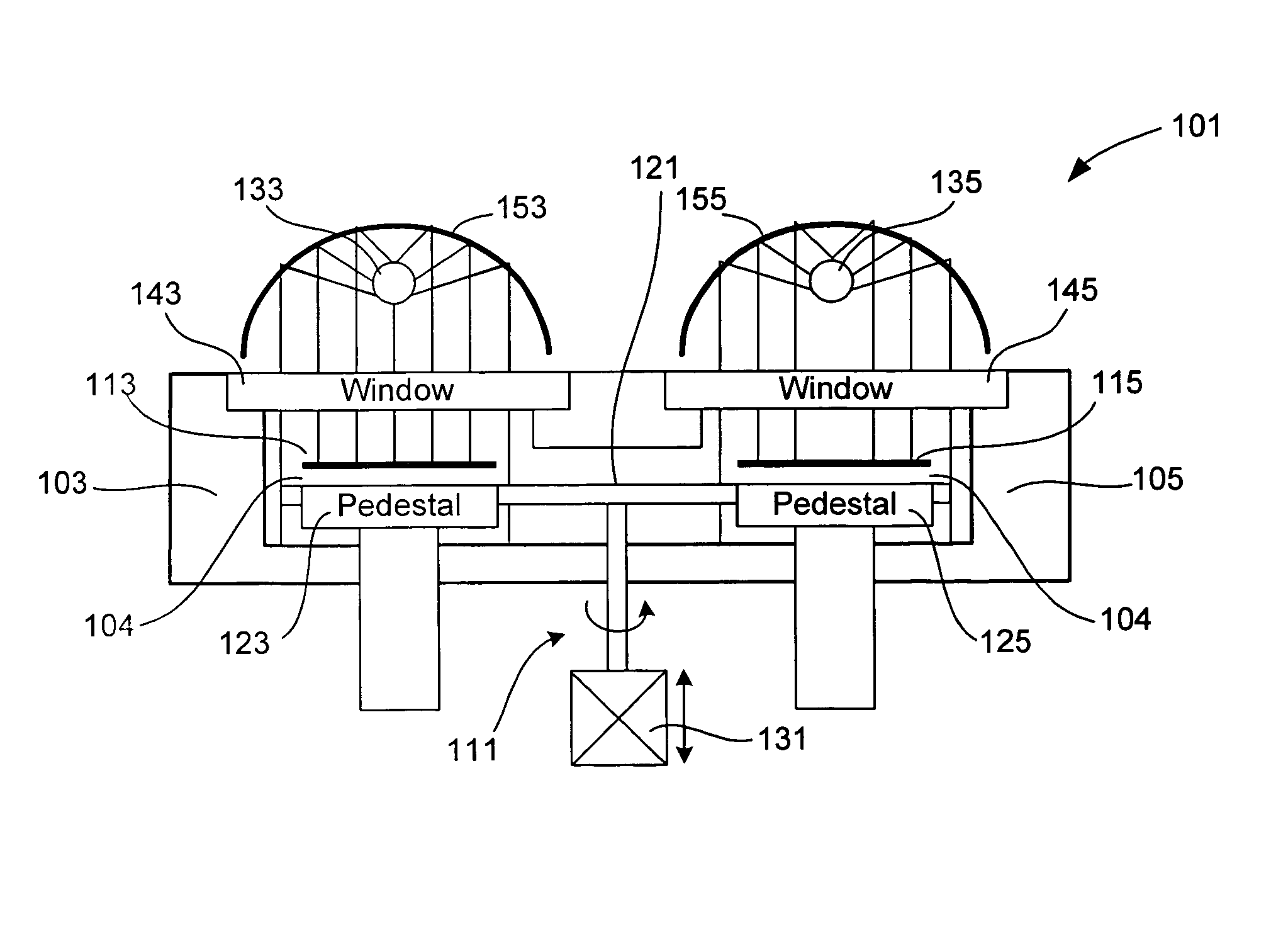
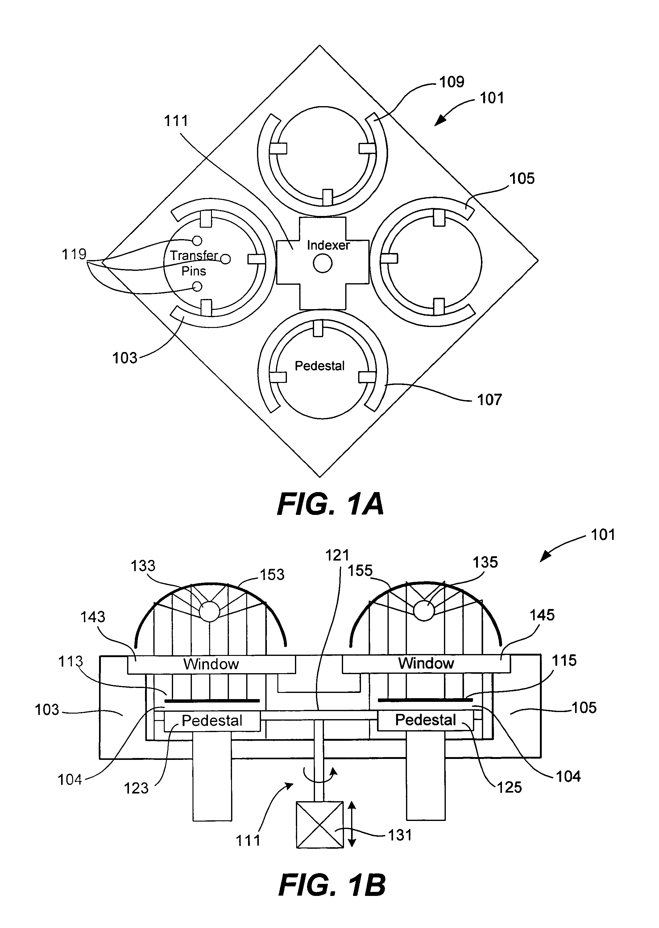
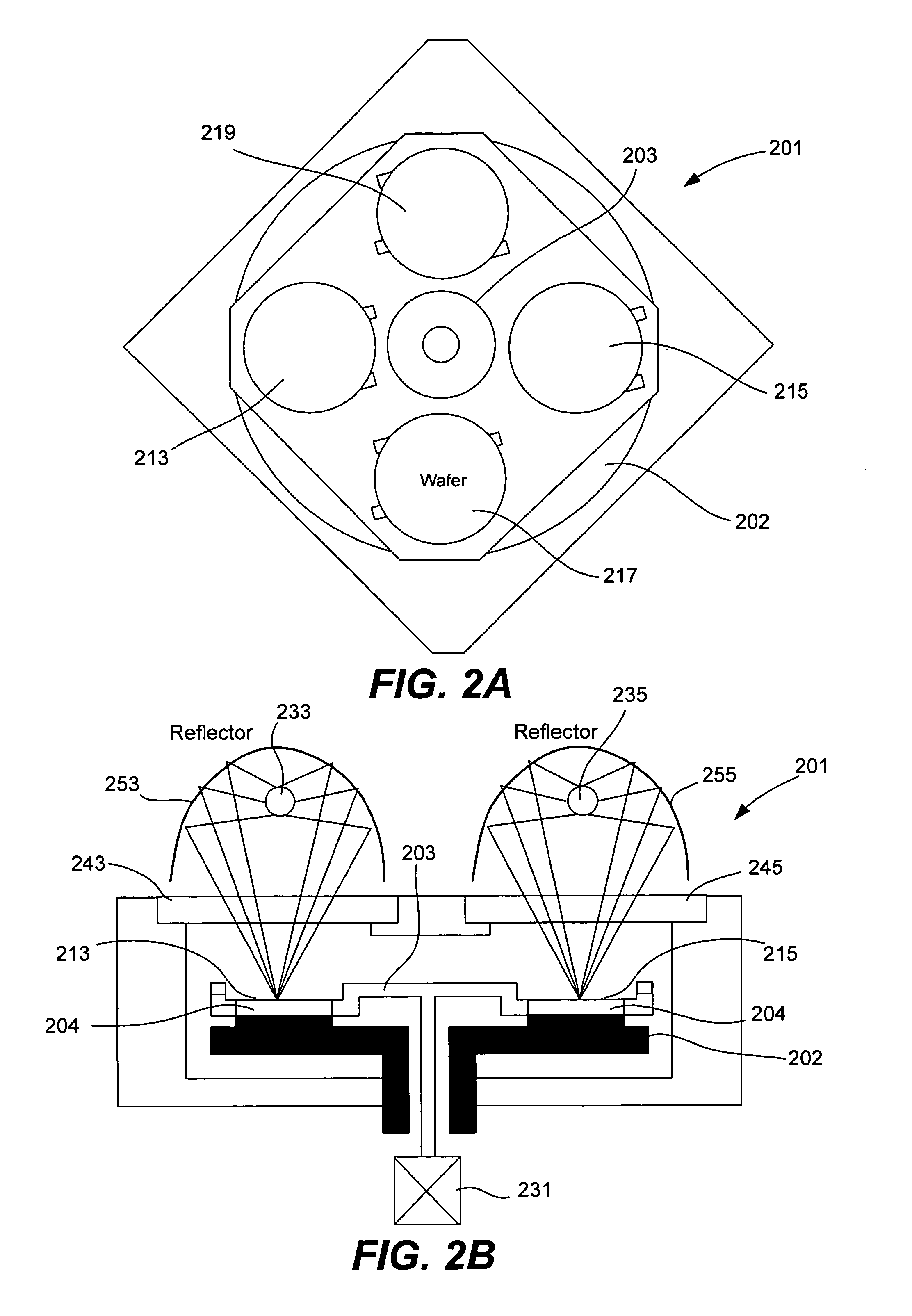
[0028]In the following detailed description of the present invention, numerous specific embodiments are set forth in order to provide a thorough understanding of the invention. However, as will be apparent to those skilled in the art, the present invention may be practiced without these specific details or by using alternate elements or processes. In other instances well-known processes, procedures and components have not been described in detail so as not to unnecessarily obscure aspects of the present invention. While the use of Ultraviolet (UV) radiation has been employed for purposes of illustrating the present invention, other forms of radiation (i.e., from other parts of the electromagnetic spectrum) can also be practiced using the same essential elements described herein.

[0029]UV curing of semiconductor wafers has many applications including removing porogens, strengthening porous OSG backbones, improving dense non-porous OSG film properties, curing nitrides and o...


PUM

PropertyMeasurementUnit
gate widthaaaaaaaaaa
temperaturesaaaaaaaaaa

Abstract

The present invention relates to curing of semiconductor wafers. More particularly, the invention relates to cure chambers containing multiple cure stations, each featuring one or more UV light sources. The wafers are cured by sequential exposure to the light sources in each station. In some embodiments, the wafers remain stationary with respect to the light source during exposure. In other embodiments, there is relative movement between the light source and the wafer during exposure. The invention also provides chambers that may be used to independently modulate the cross-linking, density and increase in stress of a cured material by providing independent control of the wafer temperature and UV intensity.

Description

BACKGROUND[0001]As IC device geometries shrink, development of low-k inter-metal dielectrics (IMDs) becomes more important. Current production processes use dense films that have a k-value between 3 and 4. These films are typically deposited using Plasma Enhanced Chemical Vapor Deposition (PECVD) processes and are typically made from either fluoro-silicate glass (FSG) or organo-silicate glass (OSG). Devices in current production range between 90 nm and 120 nm in gate width. The Semiconductor Industry roadmap calls for further shrinking these device geometries to 65 nm, then 45 nm and beyond over the remainder of this decade.[0002]As device geometries shrink further, there is a need for IMD films with k-values under 2.7. Successfully developing a film of such low capacitance requires including porosity in the film. To this end, ultra-low-k (ULK) IMD films of porous OSG have been developed. These ULK films are deposited using PECVD techniques, wherein an OSG backbone and a pore genera...

Claims


Application Information

Patent Timeline
Patent Type & Authority Patents(United States)
IPC IPC(8): C23C16/48C23C16/458C23F1/00H01L21/306C23C16/06C23C16/22
CPCC23C16/56H01L21/67115H01L21/67109
Inventor SHRINIVASAN, KRISHNAWANG, FENGKAMIAN, GEORGEGENTILE, STEVEYAM, MARK
Owner NOVELLUS SYSTEMS
Why Eureka
Try Eureka