System-in packages

a technology of system-in packages and components, applied in the direction of semiconductor devices, semiconductor/solid-state device details, electrical apparatus, etc., can solve the problems of significant challenges in manufacturability and structural reliability, and achieve good electromagnetic field shielding, high silicon utilization, and high routing density

Active Publication Date: 2012-04-24
QUALCOMM INC
View PDF8 Cites 75 Cited by
  • Summary
  • Abstract
  • Description
  • Claims
  • Application Information

AI Technical Summary

Benefits of technology

[0010]Furthermore, exemplary embodiments can provide for ease for manufacturing multi-layer chip integration with good electromagnetic field shield and high routing density between chips due to fine-pitched intra-chip metal bumps and on-chip metal bumps.
[0011]Furthermore, exemplary embodiments can provide manufacturing multi-layer chip integration with high silicon utilization.

Problems solved by technology

While WLP is a high throughput and low cost approach to IC chip packaging, it however invites significant challenges in manufacturability and structural reliability.

Method used


Image

  • System-in packages
  • System-in packages
  • System-in packages

Examples


Embodiment Construction

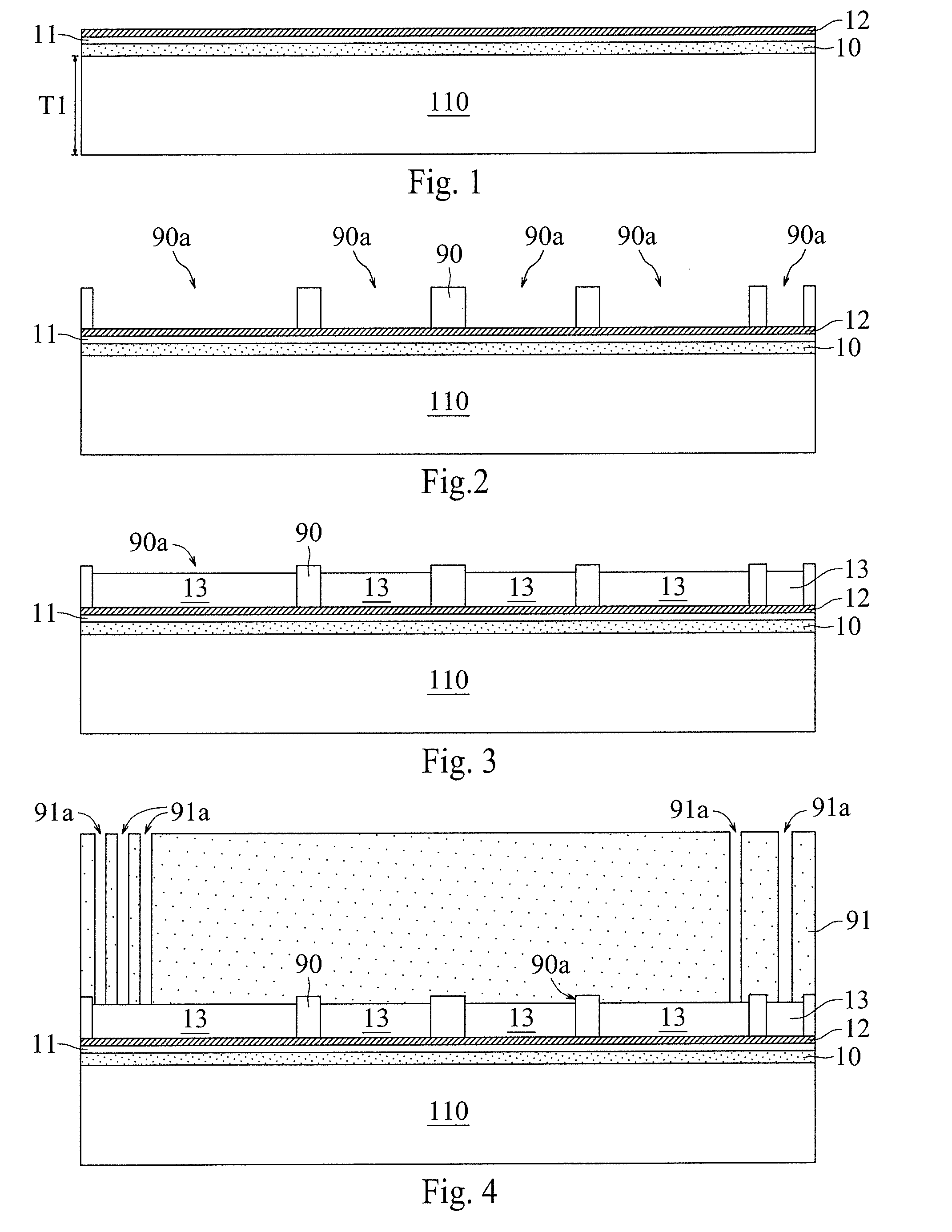
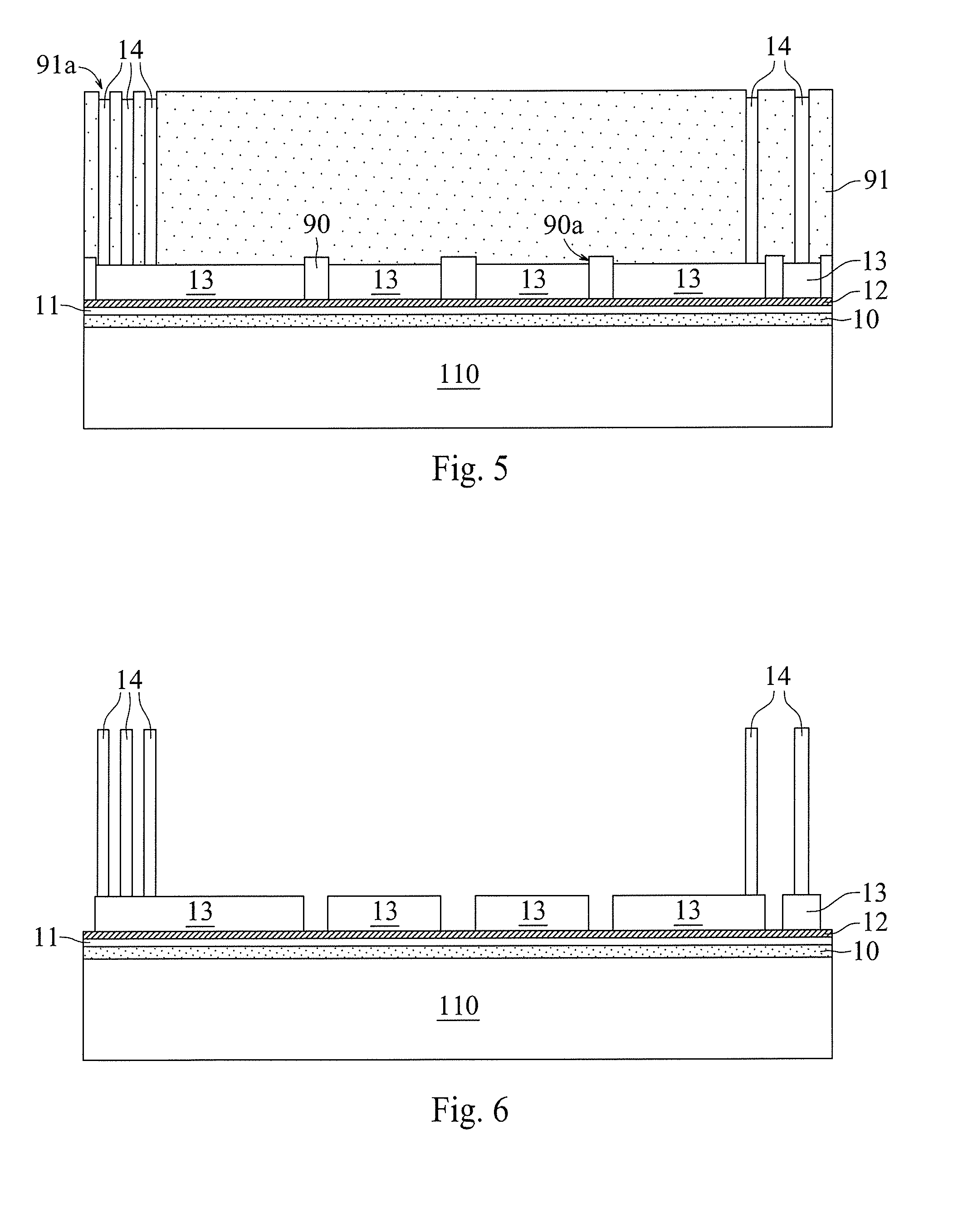
[0047]Illustrative embodiments are now described. Other embodiments may be used in addition or instead. Details that may be apparent or unnecessary may be omitted to save space or for a more effective presentation. Conversely, some embodiments may be practiced without all of the details that are disclosed.

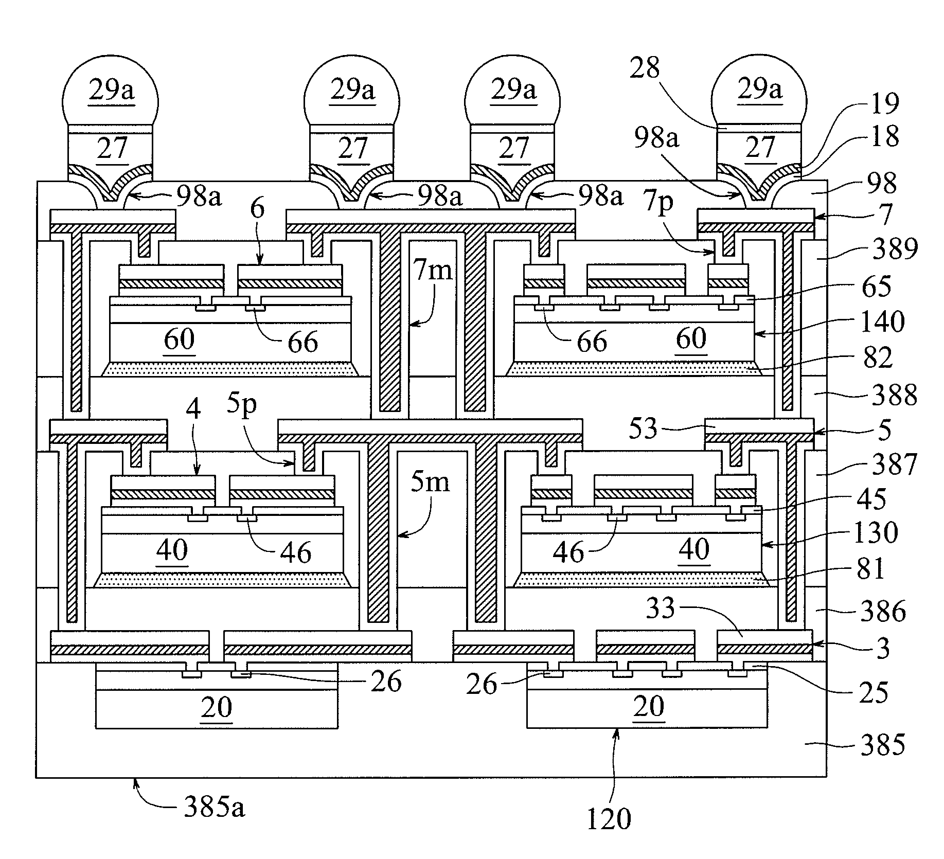
[0048]Aspects of the present disclosure are directed to system-in packages or multichip modules (MCMs) that include multi-layer chips in a multi-layer polymer structure, on-chip metal bumps on the multi-layer chips, intra-chip metal bumps in the multi-layer polymer structure, and patterned metal layers in the multi-layer polymer structure. The multi-layer chips in the multi-layer polymer structure can be connected to each other or to an external circuit or structure, such as mother board, ball-grid-array (BGA) substrate, printed circuit board, metal substrate, glass substrate and / or ceramic substrate, through the on-chip metal bumps, the intra-chip metal bumps, and / or the patterned...


PUM

PropertyMeasurementUnit
thicknessaaaaaaaaaa
thicknessaaaaaaaaaa
thicknessaaaaaaaaaa

Abstract

System-in packages, or multichip modules, are described which can include multi-layer chips in a multi-layer polymer structure, on-chip metal bumps on the multi-layer chips, intra-chip metal bumps in the multi-layer polymer structure, and patterned metal layers in the multi-layer polymer structure. The multi-layer chips in the multi-layer polymer structure can be connected to each other or to an external circuit through the on-chip metal bumps, the intra-chip metal bumps and the patterned metal layers. The system-in packages can be connected to external circuits through solder bumps, meal bumps or wirebonded wires.

Description

RELATED APPLICATION[0001]This application claims priority to U.S. provisional application No. 61 / 178,493, filed on May 14, 2009, which is herein incorporated by reference in its entirety.BACKGROUND OF THE DISCLOSURE[0002]1. Field of the Disclosure[0003]The disclosure relates to system-in packages, and more particularly, to system-in packages that utilize on-chip metal bumps and intra-chip metal bumps for electrical interconnection between stacked chips.[0004]2. Brief Description of the Related Art[0005]Semiconductor wafers are processed to produce IC (integrated circuit) chips having ever-increasing device density and shrinking feature geometries. Multiple conductive and insulating layers are required to enable the interconnection and isolation of the large number of semiconductor devices in different layers (e.g., active and passive devices, such as TFT, CMOS, capacitors, inductors, resistors, etc). Such large scale integration results in an increasing number of electrical connecti...

Claims


Application Information

Patent Timeline
Patent Type & Authority Patents(United States)
IPC IPC(8): H01L23/02
CPCH01L23/49816H01L23/5383H01L23/5384H01L23/5385H01L23/5389H01L24/24H01L24/82H01L25/0652H01L25/0655H01L25/0657H01L25/50H01L24/45H01L2224/24145H01L2224/24226H01L2224/45015H01L2224/45124H01L2224/45144H01L2224/45147H01L2224/73204H01L2225/06513H01L2225/06517H01L2225/06524H01L2225/06541H01L2924/01013H01L2924/01014H01L2924/01015H01L2924/01029H01L2924/01042H01L2924/01046H01L2924/01049H01L2924/0105H01L2924/01073H01L2924/01074H01L2924/01075H01L2924/01077H01L2924/01078H01L2924/01079H01L2924/01082H01L2924/04941H01L2924/04953H01L2924/09701H01L2924/10329H01L2924/14H01L2924/15311H01L2924/19041H01L2924/19042H01L2924/19043H01L2924/19107H01L2924/20751H01L2924/20752H01L2924/20753H01L2924/20754H01L2924/30105H01L2924/3025H01L2924/00014H01L2924/01005H01L2924/01006H01L2924/01019H01L2924/01023H01L2924/01024H01L2924/01033H01L2924/01044H01L2924/01045H01L2924/01047H01L2924/01072H01L2924/014H01L2924/01028H01L2224/24137H01L2224/32245H01L2224/73267H01L2224/92244H01L2224/8203H01L2924/10253H01L2924/00H01L2224/48465H01L2924/13091H01L2924/15788H01L2924/15787H01L2924/181H01L2924/1305H01L2224/04105H01L2224/12105H01L24/96H01L2224/32225H01L25/065H01L23/538H01L23/48H01L21/70
Inventor LIN, MOU-SHIUNGLEE, JIN-YUAN
Owner QUALCOMM INC
Why Eureka
Try Eureka