Active matrix device and method of driving the same

a technology of active matrix and drive device, which is applied in the field of digital microfluidics, can solve the problems of device degradation or failure, device voltage switching must be at least equal, and the ewod actuation voltage may still exceed the maximum voltage rating of the tfts, so as to reduce the dynamic power consumption of the device and reduce the voltage switched

Active Publication Date: 2012-05-08
SHARP LIFE SCI EU LTD
View PDF5 Cites 87 Cited by
  • Summary
  • Abstract
  • Description
  • Claims
  • Application Information

AI Technical Summary

Benefits of technology

[0042]Reducing the voltage switched by the TFT elements to the EW drive voltage also reduces the dynamic power consumption of the device in comparison to the AC drive scheme whereby the voltage of the top substrate is maintained at a constant potential.

Problems solved by technology

LC displays generally require that the voltage across the liquid crystal should be alternated (“inversion”) since the application of a DC field has deleterious effects for the LC material.
A disadvantage of U.S. Pat. No. 7,163,612 (J. Sterling et al.
This has the disadvantage that the voltages switched by the TFTs must be at least equal to the electrowetting drive voltage.
In some cases however, the EWOD actuation voltage may still exceed the maximum voltage rating of the TFTs.
High voltage operation of TFTs may result in device degradation or failure as is well known.
A further disadvantage of the high operating voltage is that power consumption from operating the switches (due to the charging and discharging of the parasitic switch capacitance) may also be significant.

Method used


Image

  • Active matrix device and method of driving the same
  • Active matrix device and method of driving the same
  • Active matrix device and method of driving the same

Examples


first embodiment

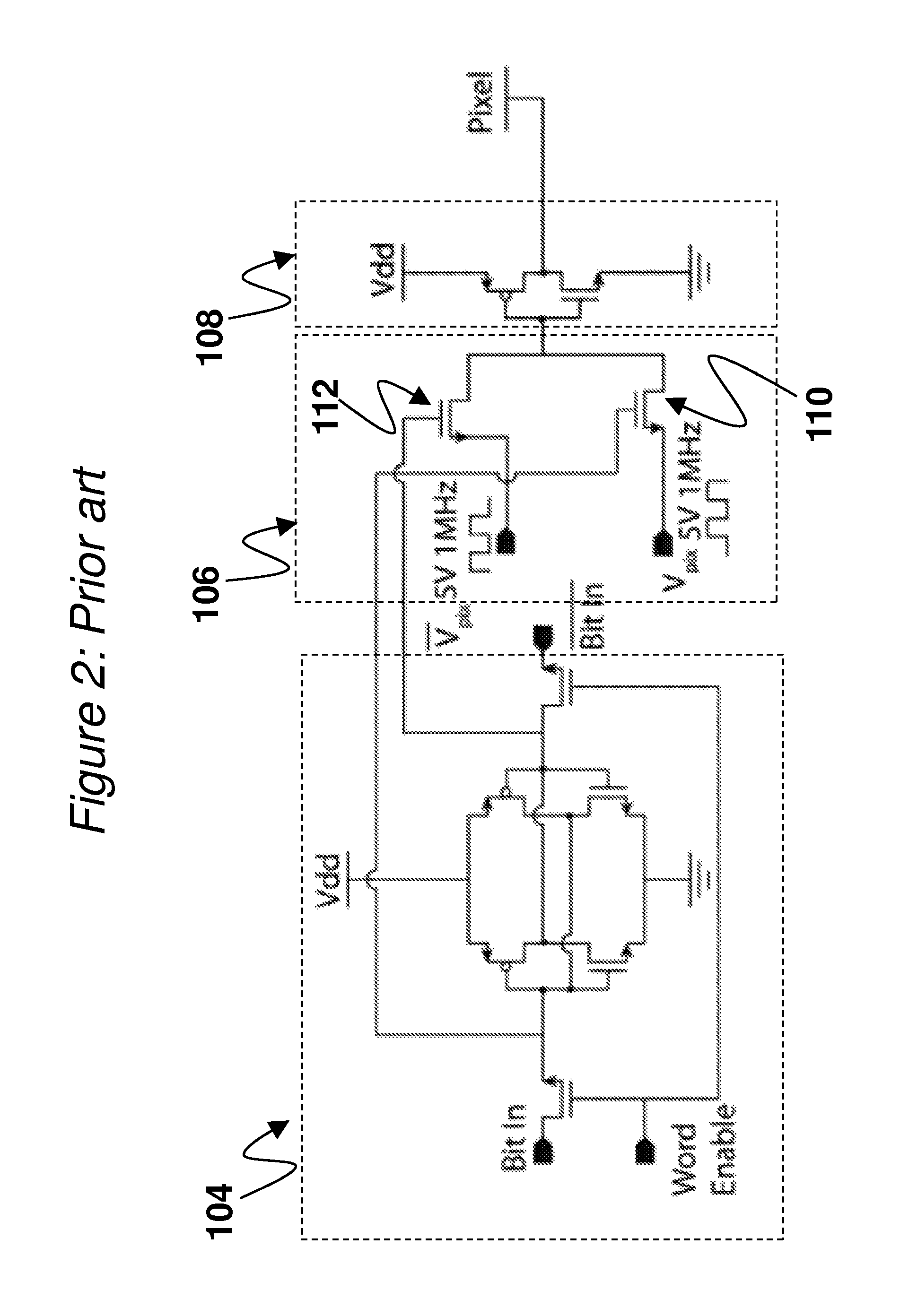
[0091]The array element circuit 84 is shown in FIG. 6. The remainder of the AM-EWOD device is of the standard construction previously described and includes a top substrate 36 having an electrode 28.

[0092]Each array element circuit 84 is arranged so as to supply the electrowetting drive voltage VEW across the liquid droplet 4 and includes the following components:[0093]A memory function 222 comprising:[0094]A column write line COL (originating from the column driver 78), which may be common to array elements within the same column[0095]A row select line ROW (originating from the row driver 76), which may be common to array elements within the same row[0096]A storage capacitor 203[0097]A DC supply voltage Vref[0098]A switch transistor 206[0099]An inversion circuit 224 comprising:[0100]A first analogue switch 214[0101]A second analogue switch 216[0102]A supply voltage V1, which may be common to all elements within the array[0103]A second supply voltage V2, which may be common to all ...

second embodiment

[0146]The operation of this embodiment is as described for the This embodiment has the additional advantage that by replacing the single SRAM switch transistors 206,230 by analogue switches 240,242, problems due to threshold voltage drop in the SRAM cell may be avoided.

fourth embodiment

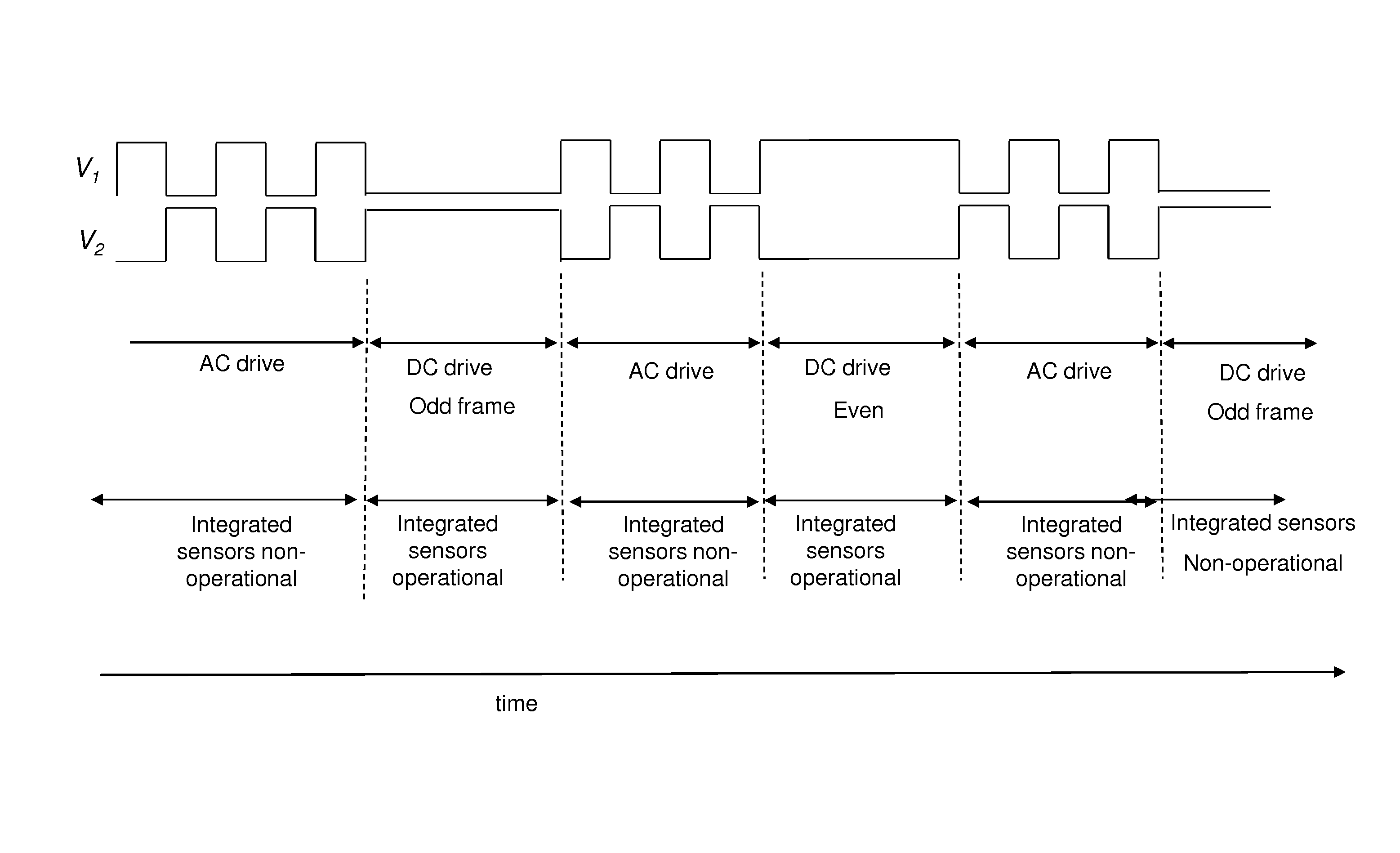
[0147]According to the present invention, the AM-EWOD device is that of any of the previous embodiments with the exception of a modified driving method whereby the AC voltage signal applied to the electrode 28 of the top substrate 36 has an increased amplitude.

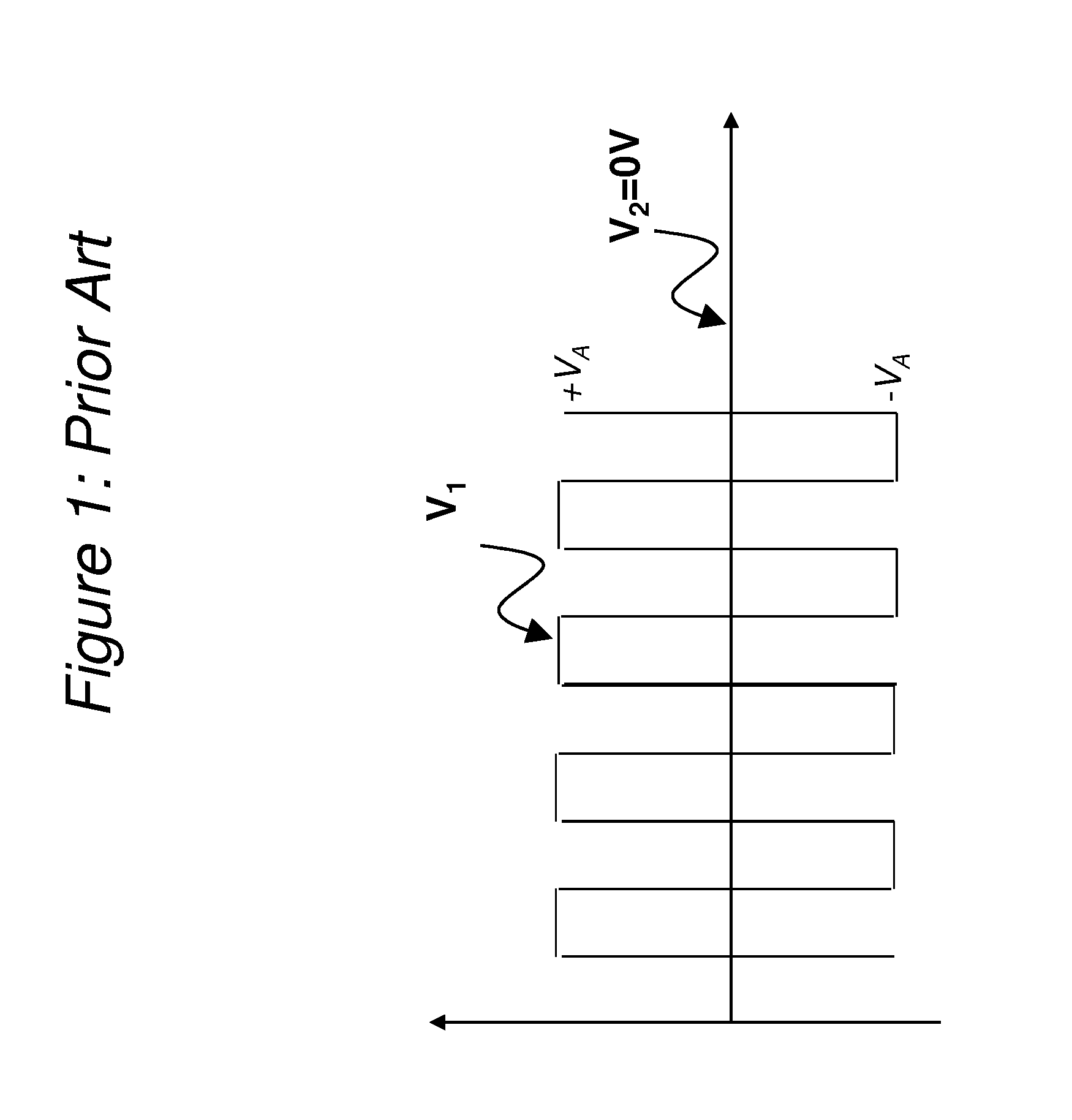
[0148]Specifically the array element circuit 84, realised in thin-film electronics 74 on the lower substrate 72, is arranged to switch either supply voltage V1 or supply voltage V2 to the EW drive electrode 38 as described for the previous embodiments. Referring to FIG. 10:[0149]Supply voltage V1 consists of a square wave voltage pulse of amplitude VB and period t0. For convenience of description in what follows we may define V1 as having low level 0V, and high level VB.[0150]Supply voltage V2 is the logical inverse of V1, i.e., consists of a square wave voltage pulse of amplitude VB and period t0. The low level of V2 is 0V, the high level VB, and V2 is in anti-phase to V1.

A supply voltage V3 is applied to the electrode 28 of ...


PUM

PropertyMeasurementUnit
drive frequenciesaaaaaaaaaa
frequencyaaaaaaaaaa
actuation voltagesaaaaaaaaaa

Abstract

An active matrix electrowetting on dielectric (AM-EWOD) device which includes a plurality of array elements configured to manipulate one or more droplets of fluid on an array, each of the array elements including a corresponding array element circuit. Each array element circuit includes a top substrate electrode and a drive electrode between which the one or more droplets may be positioned; circuitry configured to write data to the corresponding array element by selectively applying to the drive electrode either: (i) a time-varying voltage waveform V1 of amplitude VB and period t0; or (ii) a time-varying voltage waveform V2, the logical inverse of V1, and applying to the top substrate electrode the time-varying voltage waveform V2+Voffset, where Voffset represents an offset voltage signal which may have AC and/or DC components and may equal zero.

Description

TECHNICAL FIELD[0001]The present invention relates to active matrix arrays and elements thereof.[0002]In a particular aspect, the present invention relates to digital microfluidics, and more specifically to Active Matrix Electrowetting-On-Dielectric (AM-EWOD). Electrowetting-On-Dielectric (EWOD) is a known technique for manipulating droplets of fluid on an array. Active Matrix EWOD (AM-EWOD) refers to implementation of EWOD in an active matrix array, for example by using thin film transistors (TFTs). The invention further relates to methods of driving such a device.BACKGROUND ART[0003]Electrowetting on dielectric (EWOD) is a well known technique for manipulating droplets of fluid by application of an electric field. It is thus a candidate technology for digital microfluidics for lab-on-a-chip technology. An introduction to the basic principles of the technology can be found in “Digital microfluidics: is a true lab-on-a-chip possible?”, R. B. Fair, Microfluid Nanofluid (2007) 3:245-2...

Claims


Application Information

Patent Timeline
Patent Type & Authority Patents(United States)
IPC IPC(8): G01N27/447G01N27/453
CPCB01L3/50273G02B26/005G09G3/348B01L2200/0673B01L2300/161G09G2310/068G09G2300/0857B01L2400/0427
Inventor HADWEN, BENJAMIN JAMESJACOBS, ADRIAN MARC SIMONHECTOR, JASON RODERICKJOHN, GARETH
Owner SHARP LIFE SCI EU LTD
Why Eureka
Try Eureka