Patterning methods for stretchable structures

a technology of stretchable structures and patterning methods, applied in the field of microfabrication processing techniques, can solve problems such as the breakage of long polymer chains by bonding

Active Publication Date: 2012-05-29
THE BOARD OF TRUSTEES OF THE UNIV OF ILLINOIS
View PDF61 Cites 7 Cited by
  • Summary
  • Abstract
  • Description
  • Claims
  • Application Information

AI Technical Summary

Benefits of technology

[0018]In a specific embodiment, the exposing steps are carried out using a fluence of ablation radiation selected over the range of 30 mJ / cm2 to 500 mJ / cm2 and / or using ablation radiation having wavelengths selected over the range of 100 nm to 400 nm. In specific embodiments, the ablation radiation is excimer laser radiation, such as radiation from a F2, ArF, KrF, XeCl or XeF excimer laser; ion laser radiation, such as from an Ar, Kr, or Cd ion laser; or frequency-multiplied solid state laser radiation, such as from a Nd:YAG or Nd:Glass laser. In a specific embodiment, the ablation radiation does not ablate or does not significantly ablate the patterned metal layers during the exposing step; that is, the patterned metal layers remain intact or substantially intact after and during the exposure to the ablation radiation. In a specific embodiment, the ablation radiation does not damage or does not significantly damage the patterned metal layers during the exposing step.

Problems solved by technology

When the focused optical patterns strike the substrate, the polymer absorbs the energy, which causes bond breaking of the long polymer chains.

Method used


Image

  • Patterning methods for stretchable structures
  • Patterning methods for stretchable structures
  • Patterning methods for stretchable structures

Examples


example 1

Applications of and Processes for Creating Stretchable Structures

[0078]Stretchable, large-area, sensor arrays provide multimodal sensory information about the environment, such as temperature, pressure, strain, and chemical composition. These sensor arrays find applications in aerospace and infrastructure structural health monitoring, tactile sensors for robotics and electronic textiles for patient, soldier, and athlete physical health monitoring. Furthermore, the new fabrication methods described herein for large-area sensors focus on low-cost and reliability, and therefore permit the development of new low-cost sensors for consumer applications.

[0079]Stretchable structures may be used for flexible electronics, display applications, and electronics packaging applications. These applications usually contain multiple layer of interconnects that interface between different chip packages. In these applications, there is a need for robust and conformable electronics for the various appl...

example 2

Stretchable and Flexible Interconnects

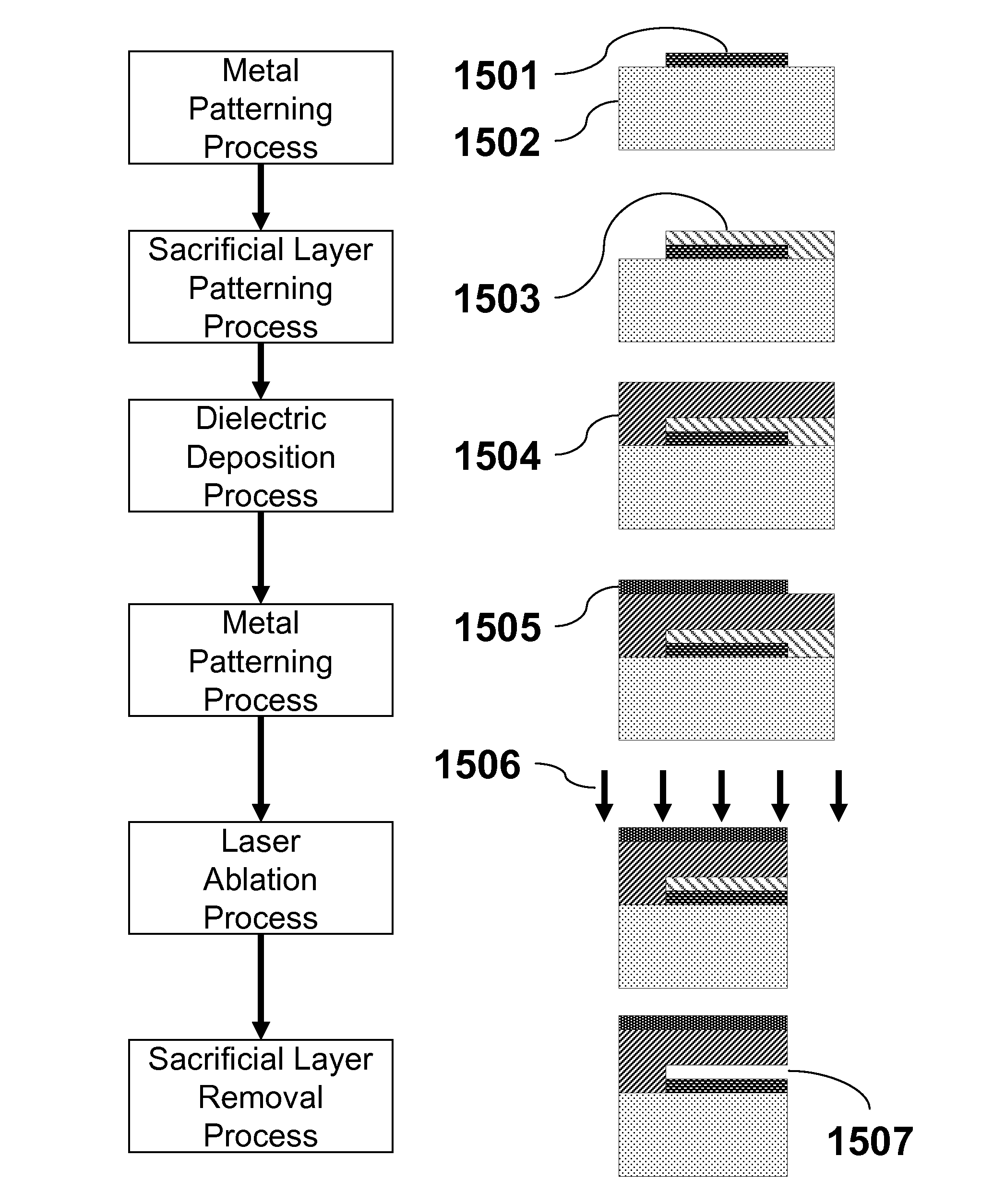
[0089]Interconnects relay the signal from a sensor output to the external environment. For sensor skins, because of the large number of elements, it is important to have multiple layers of interconnects. In one embodiment, shown in FIG. 11A, at least two layers of interconnects are present. These layers of interconnects may be perpendicular to each other; one interconnect layer 1101 probes the bottom electrodes of a number capacitive sensors 1102 while the other interconnect layer 1103 probes the top electrodes. The interconnects are arranged in a row / column fashion such that a unique sensor or actuator can be probed by selecting a row and column. It is advantageous to have a high electrical-conductivity interconnect to minimize the time delay between probes and to maximize the sensor throughput; therefore, aluminum is utilized as the interconnect material. High-conductivity metals such as aluminum, gold, and copper are commercially used for int...

example 3

Capacitive Sensors

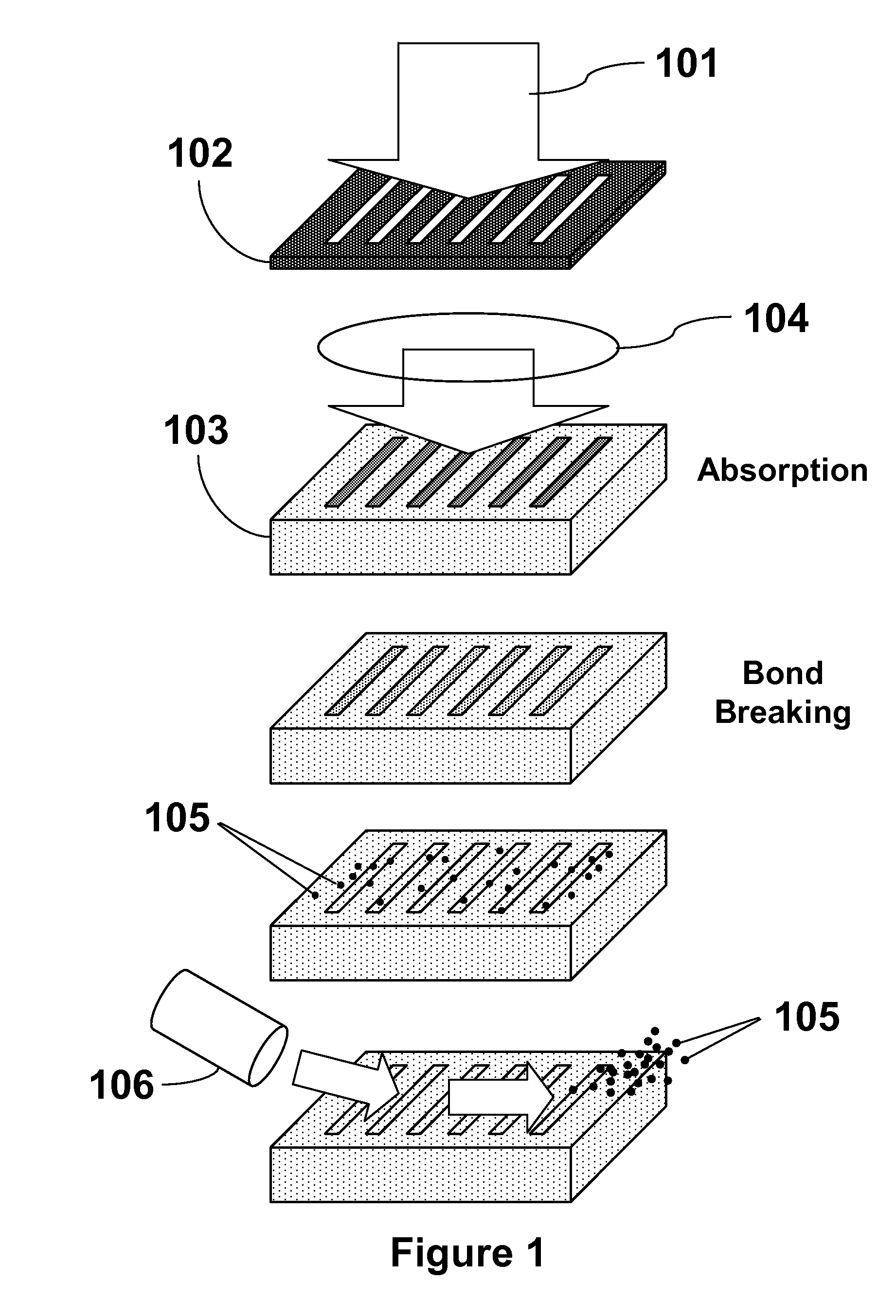
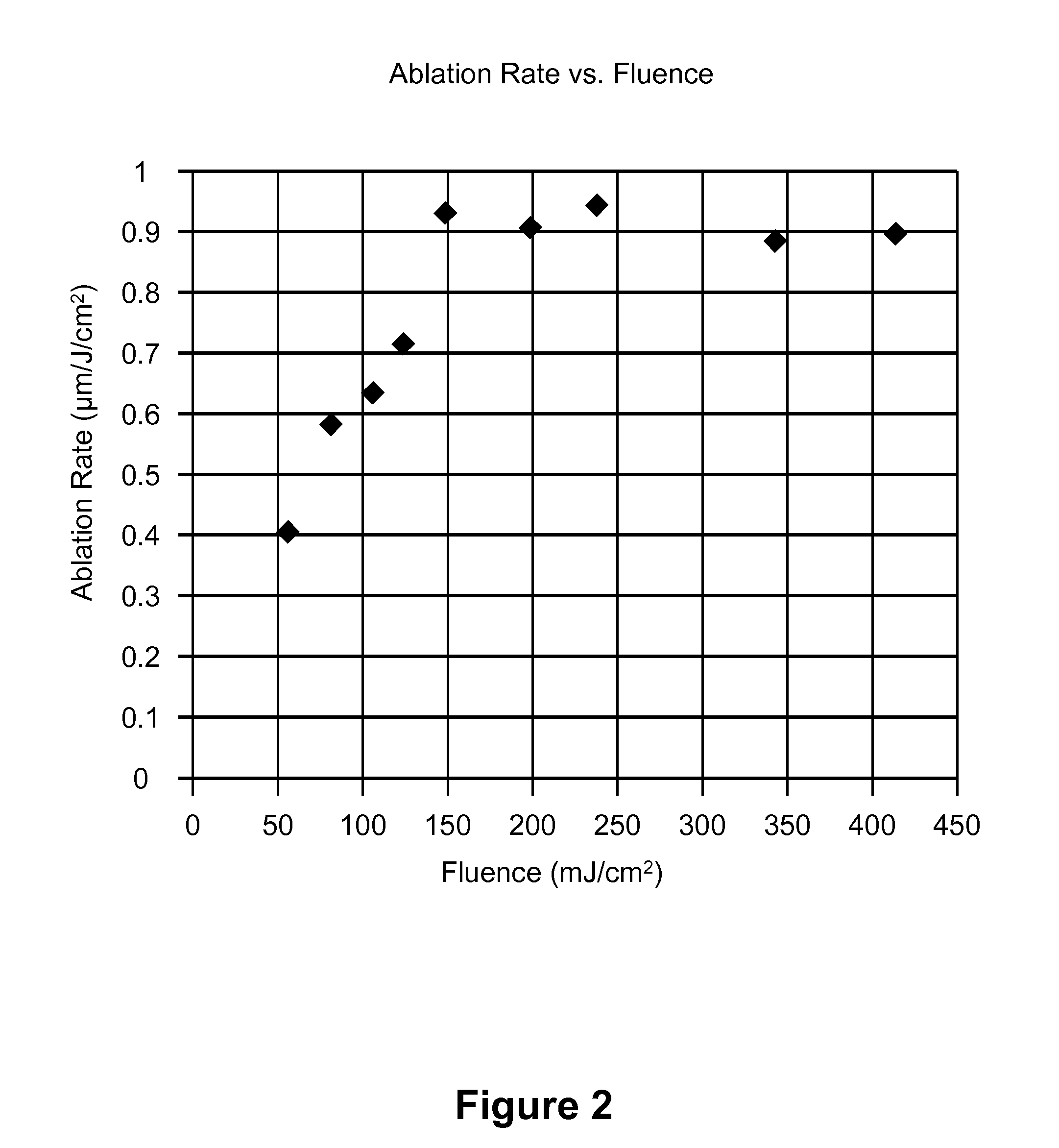
[0092]Described in this example is a fabrication process embodiment for the fabrication of capacitive sensors. Capacitive sensors have two metal electrodes which can act as in-situ metal masks this fabrication process. Capacitive sensors rely on an environmental factor to change the sensed capacitance. Capacitance is a function of area of the capacitive plates, the distance between the plates, and the dielectric constant of the material between the two plates, so a change of any of these parameters will change the sensed capacitance.

[0093]Several common capacitive sensors are pressure sensors, accelerometers, and temperature / humidity sensors. Pressure sensors work as follows: a force from an applied pressure imparts a stress on the polymer, distorts the diaphragm, and decreases the distance between two capacitive plates which increases the sensed capacitance correspondingly. Likewise, capacitive accelerometers transduce a change in force through a change in the cap...


PUM

PropertyMeasurementUnit
thicknessaaaaaaaaaa
thicknessaaaaaaaaaa
thicknessaaaaaaaaaa

Abstract

Described herein are processing techniques for fabrication of stretchable and / or flexible electronic devices using laser ablation patterning methods. The laser ablation patterning methods utilized herein allow for efficient manufacture of large area (e.g., up to 1 mm2 or greater or 1 m2 or greater) stretchable and / or flexible electronic devices, for example manufacturing methods permitting a reduced number of steps. The techniques described herein further provide for improved heterogeneous integration of components within an electronic device, for example components having improved alignment and / or relative positioning within an electronic device. Also described herein are flexible and / or stretchable electronic devices, such as interconnects, sensors and actuators.

Description

CROSS REFERENCE TO RELATED APPLICATION[0001]Not Applicable.BACKGROUND OF THE INVENTION[0002]This invention is in the field of microfabrication processing techniques. This invention relates generally to patterning methods for fabrication of flexible and / or stretchable electronic devices, interconnects and sensors. This invention relates to fabrication of stretchable and / or flexible structures for the production of large-area electronic products such as, micro-electro-mechanical systems (MEMS) sensor arrays, flexible printed circuit boards, electronics packaging, and other systems that require large-area structural patterning and a stretchable structure.[0003]Photoablation describes the removal of materials using high photon energies (i.e. short wavelengths, and not necessarily high intensities) and is a very effective method of patterning polymers. Typically, ultraviolet (UV) light strikes the polymer at moderate intensities such that the combination of photochemical and photothermal...

Claims


Application Information

Patent Timeline
Patent Type & Authority Patents(United States)
IPC IPC(8): G03F7/00G03F7/20G01B7/16G01P15/125
CPCB23K26/409B81C1/0019H05K1/0283B81B2201/0292B81B2203/0109B81B2207/07H05K3/0032H05K3/007H05K2201/09109H05K2203/0554H05K2203/308B23K26/40B23K2103/172
Inventor JAIN, KANTILIN, KEVIN
Owner THE BOARD OF TRUSTEES OF THE UNIV OF ILLINOIS
Why Eureka
Try Eureka