Semiconductor device and method for driving the same

a technology of semiconductors and dielectric devices, applied in the direction of pulse generators, pulse techniques, electronic switching, etc., can solve the problems of difficult to obtain enhancement type characteristics and off types, and achieve excellent reverse voltage characteristics

Active Publication Date: 2012-06-19
PANASONIC CORP
View PDF18 Cites 7 Cited by
  • Summary
  • Abstract
  • Description
  • Claims
  • Application Information

AI Technical Summary

Benefits of technology

[0066]With the semiconductor device of the present invention and the method for driving the same, it is possible to realize a semiconductor device which has excellent reverse voltage characteristics, which as a single element constitutes a bidirectional switch product, and which allows for the application of a high gate voltage, and a method for driving the same.

Problems solved by technology

However, even if a nitride semiconductor is undoped, spontaneous polarization and piezoelectric polarization produce a high concentration of carriers at the heterojunction interface.
Therefore, when an FET is produced by using a nitride semiconductor, it is likely to be of the depression type (normally-on type), and it is difficult to obtain characteristics of the enhancement type (normally-off type) (see, for example, Patent Document 1).

Method used


Image

  • Semiconductor device and method for driving the same
  • Semiconductor device and method for driving the same
  • Semiconductor device and method for driving the same

Examples


first embodiment

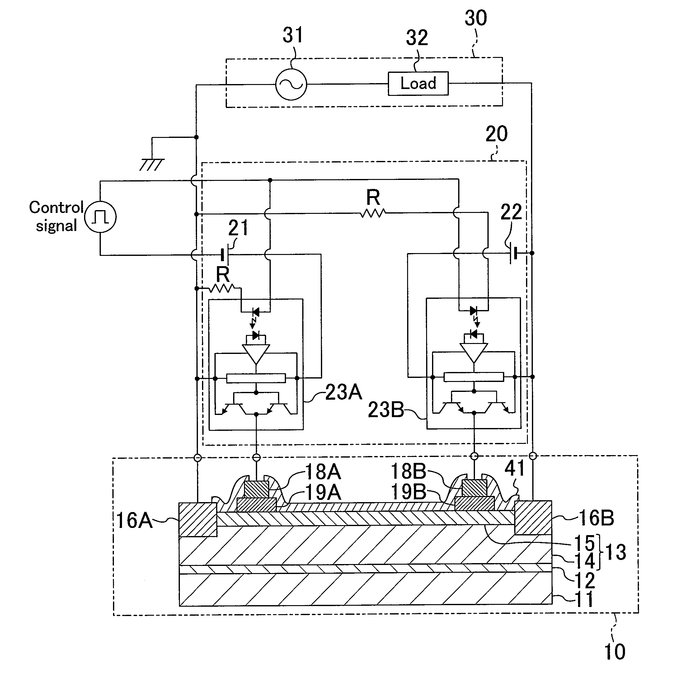
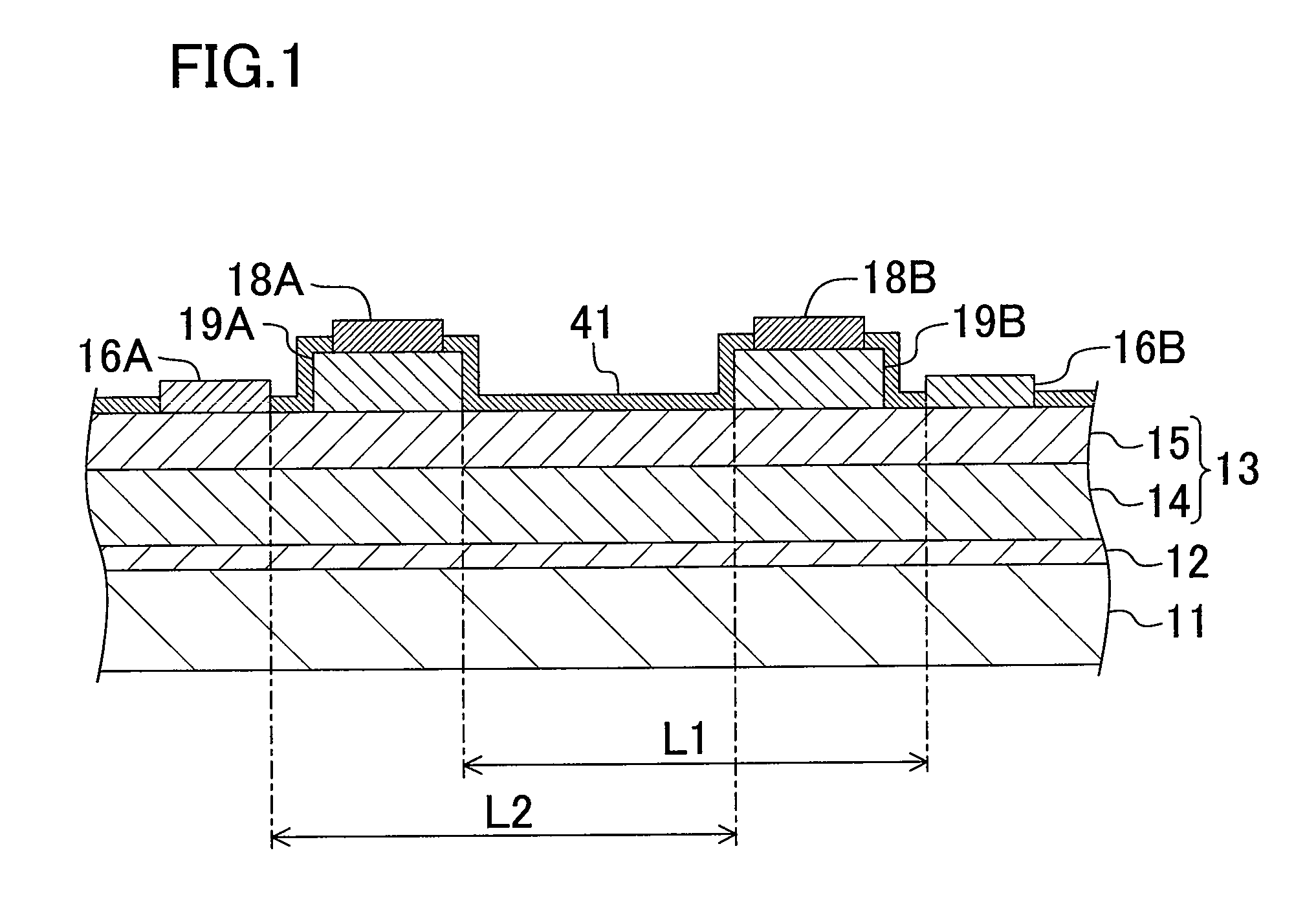
[0099]A first embodiment of the present invention will be described with reference to the drawings. FIG. 1 shows a cross section of a nitride semiconductor device according to the first embodiment of the present invention. As shown in FIG. 1, the semiconductor device of the present embodiment is a dual-gate semiconductor element. Specifically, a buffer layer 12 of AlN having a thickness of 100 nm is formed on a substrate 11 of sapphire in which the orientation of the principal plane is (0001), and a semiconductor layer stack 13 is formed thereon. The semiconductor layer stack 13 includes a first semiconductor layer 14 of undoped GaN having a thickness of 1 μm and a second semiconductor layer 15 of undoped Al0.15Ga0.85N having a thickness of 25 nm, which are formed in this order from the bottom.

[0100]A first electrode 16A and a second electrode 16B are formed from a stack of titanium (Ti) and aluminum (Al) so as to be spaced apart from each other on the second semiconductor layer 15,...

second embodiment

[0117]A second embodiment of the present invention will now be described with reference to the drawings. FIG. 4 shows a cross section of a semiconductor device of the second embodiment. In FIG. 4, like elements to those of FIG. 3 are denoted by like reference numerals and will not be further described below.

[0118]As shown in FIG. 4, the semiconductor device of the present embodiment includes a third semiconductor layer 17 of p-type doped Al0.2Ga0.8N having a thickness of 15 nm between the second semiconductor layer 15 and the first control layer 19A and the second control layer 19B.

[0119]The first control layer 19A and the second control layer 19R are typically formed by forming a nitride semiconductor layer of p-type GaN on the second semiconductor layer 15 and then selectively etching the p-type nitride semiconductor layer by dry etching using a chlorine gas, for example. However, it is very difficult to completely remove by etching only the p-type nitride semiconductor layer to b...

third embodiment

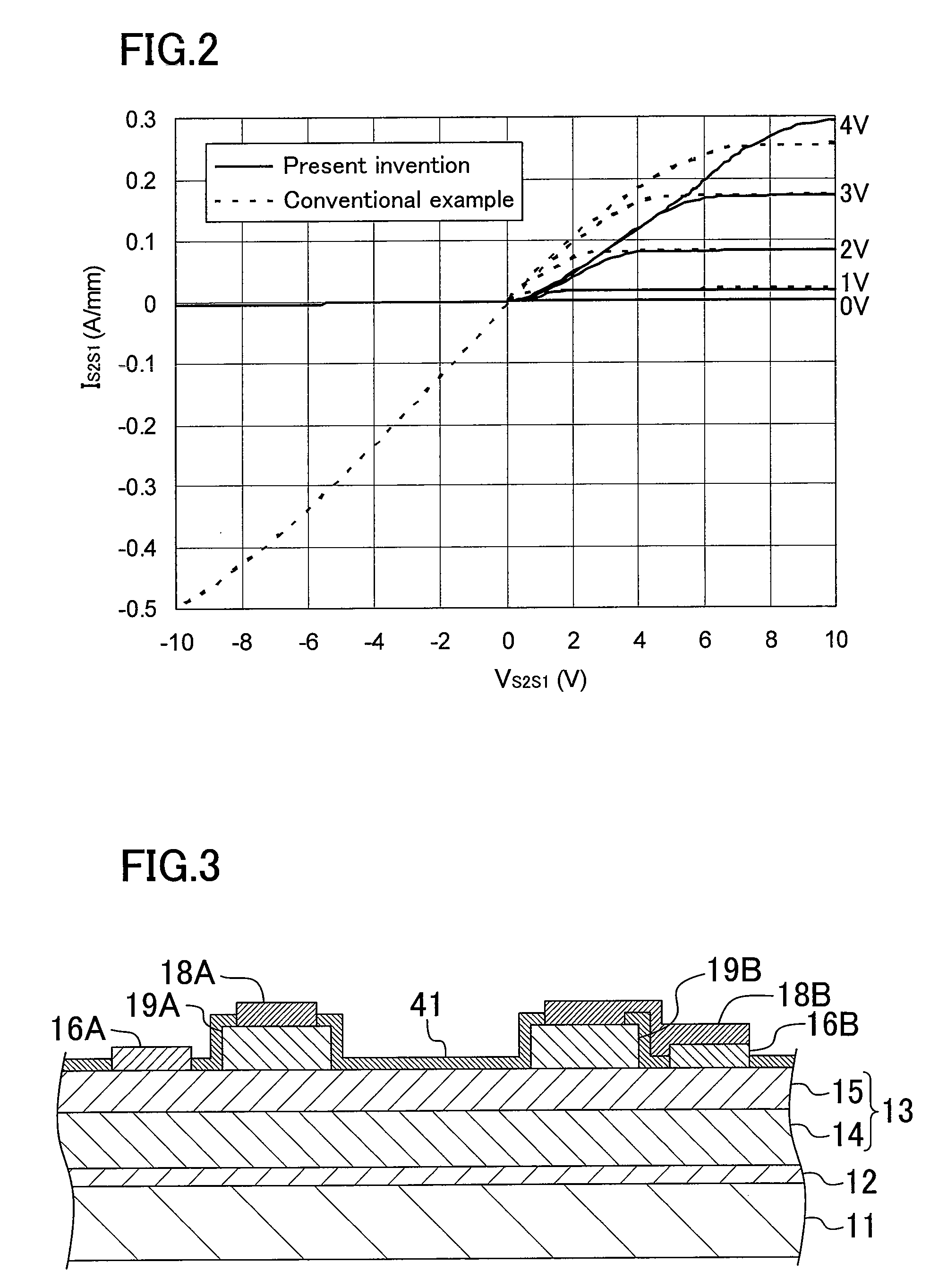
[0122]A third embodiment of the present invention will now be described with reference to the drawings. FIG. 5 shows a cross section of a semiconductor device of the third embodiment. In FIG. 5, like elements to those of FIG. 1 are denoted by like reference numerals and will not be further described below. As shown in FIG. 5, the semiconductor device of the present embodiment includes an integral electrode 16C of Ni on the second control layer 19B, wherein the integral electrode 16C is an integration of the second gate electrode and the second electrode.

[0123]FIG. 6 shows the VS2S1-IS2S1 characteristics of the semiconductor device of the present embodiment, in comparison with those of the conventional semiconductor device with no second control layer. In FIG. 6, VS2S1 is a voltage with respect to the first electrode 16A, and IS2S1 along the vertical axis is plotted assuming the positive direction is the direction of a current flow from the second electrode 16B toward the first elect...


PUM


Abstract

A semiconductor device includes a semiconductor layer stack 13 formed on a substrate 11 and having a channel region, a first electrode 16A and a second electrode 16B formed spaced apart from each other on the semiconductor layer stack 13, a first gate electrode 18A formed between the first electrode 16A and the second electrode 16B, and a second gate electrode 18B formed between the first gate electrode 18A and the second electrode 16B. A first control layer 19A having a p-type conductivity is formed between the semiconductor layer stack 13 and the first gate electrode 18A.

Description

RELATED APPLICATIONS[0001]This application is the U.S. National Phase under 35 U.S.C. §371 of International Application No. PCT / JP2007 / 072476, filed on Nov. 20, 2007, which in turn claims the benefit of Japanese Application Nos. 2006-312502, filed on Nov. 20, 2006, 2006-334094, filed on Dec. 12, 2006, and 2007-153031, filed on Jun. 8, 2007, the disclosures of which Applications are incorporated by reference herein.TECHNICAL FIELD[0002]The present invention relates to a semiconductor device, and more particularly to a semiconductor device capable of a bidirectional switching operation used for power control, and a method for driving the same.BACKGROUND ART[0003]In recent years, field effect transistors (FETs) using a nitride semiconductor such as gallium nitride (GaN) have been widely researched as power switching devices. Since GaN can form various compound materials with aluminum nitride (AlN) and indium nitride (InN), nitride semiconductors can form heterojunctions as do arsenic-b...

Claims


Application Information

Patent Timeline
Patent Type & Authority Patents(United States)
IPC IPC(8): H03K17/687
CPCH01L27/0605H01L29/739H01L29/7787H01L29/0619H01L29/1066H01L29/8124H01L29/432H01L29/2003
Inventor MORITA, TATSUOYANAGIHARA, MANABUISHIDA, HIDETOSHIUEMOTO, YASUHIROUENO, HIROAKITANAKA, TSUYOSHIUEDA, DAISUKE
Owner PANASONIC CORP
Why Eureka
Try Eureka