Victim net crosstalk reduction

a net and victim technology, applied in the field of signal networking, can solve the problems of large increased complexity of interconnect systems for such ics, and reduced geometries, so as to avoid analysis iterations and reduce the effect of crosstalk noise of coupled nets

Inactive Publication Date: 2012-06-19
MACOM CONNECTIVITY SOLUTIONS LLC
View PDF12 Cites 150 Cited by
  • Summary
  • Abstract
  • Description
  • Claims
  • Application Information

AI Technical Summary

Benefits of technology

[0017]Described herein are a system and design method for reducing the crosstalk noise of coupled nets by addressing the physical design of a system-on-chip (SoC), without relocating or modifying the actual components of the affected nets. The simultaneous switching of the aggressor and victim nets is avoided by changing the timing windows of

Problems solved by technology

The size, complexity, and operating or switching speeds of semiconductor ICs have increased, while feature geometries have decreased, and interconnect systems for such ICs have dramatically increased in complexity.
In many situations these factors have increased the possible impact on timing due to noise resulting from parasitic capacitance within the interconnect system.
To the first order, only two kinds of timing errors are possible in such a system.
First, a hold time violation may occur, when an input signal changes too quickly after the clock's active transition.
Second, a setup time violation may occur when a signal arrives too late, and misses the time when it should advance.
While such timing measurements can theoretically be performed using a rigorous circuit simulation, such an approach is liable to be too slow to be practical.
Faster design times are a result of using simplified STA delay models, and a limited consideration of the effects of logical interactions between signals.
Also, since STA is capable of verifying every path, apart from helping locate setup and

Method used


Image

  • Victim net crosstalk reduction
  • Victim net crosstalk reduction
  • Victim net crosstalk reduction

Examples


Embodiment Construction

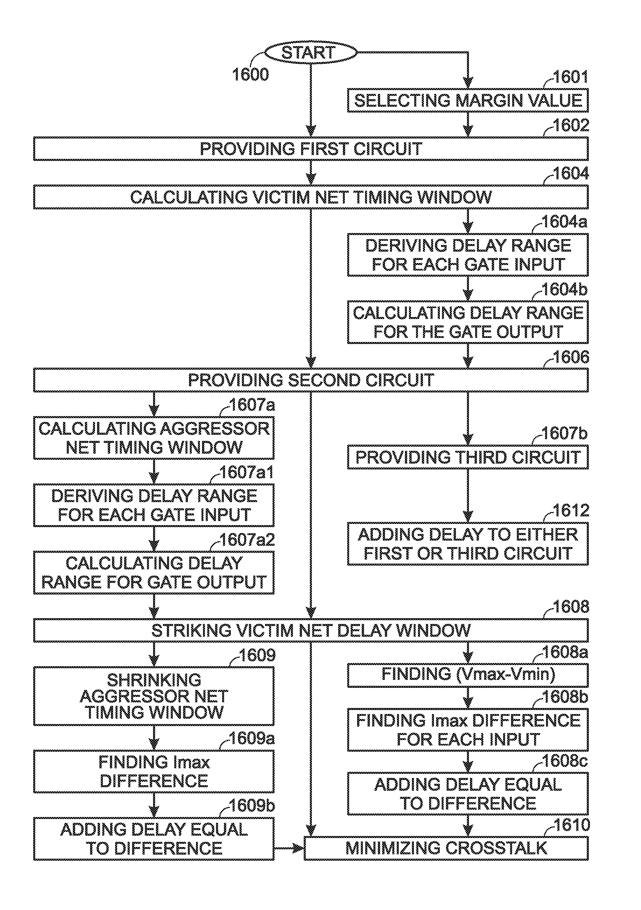
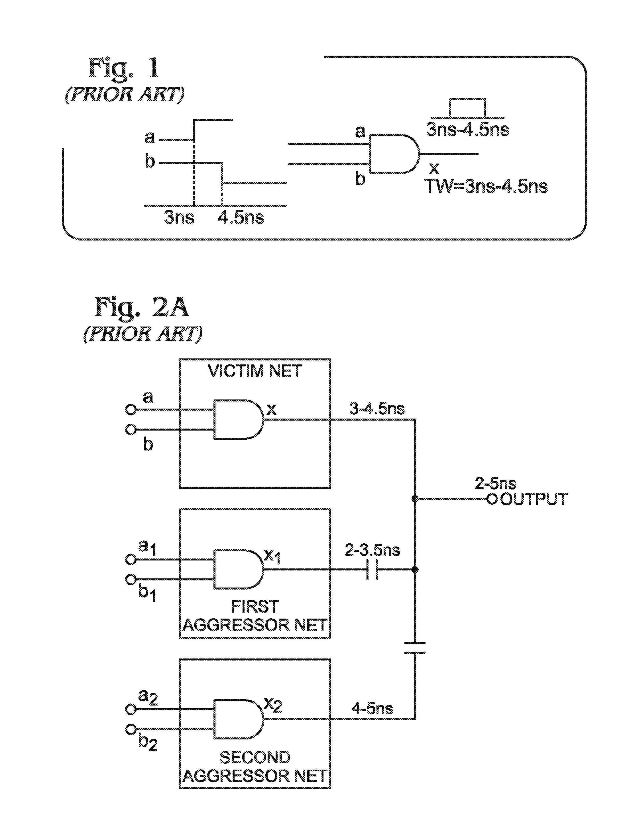
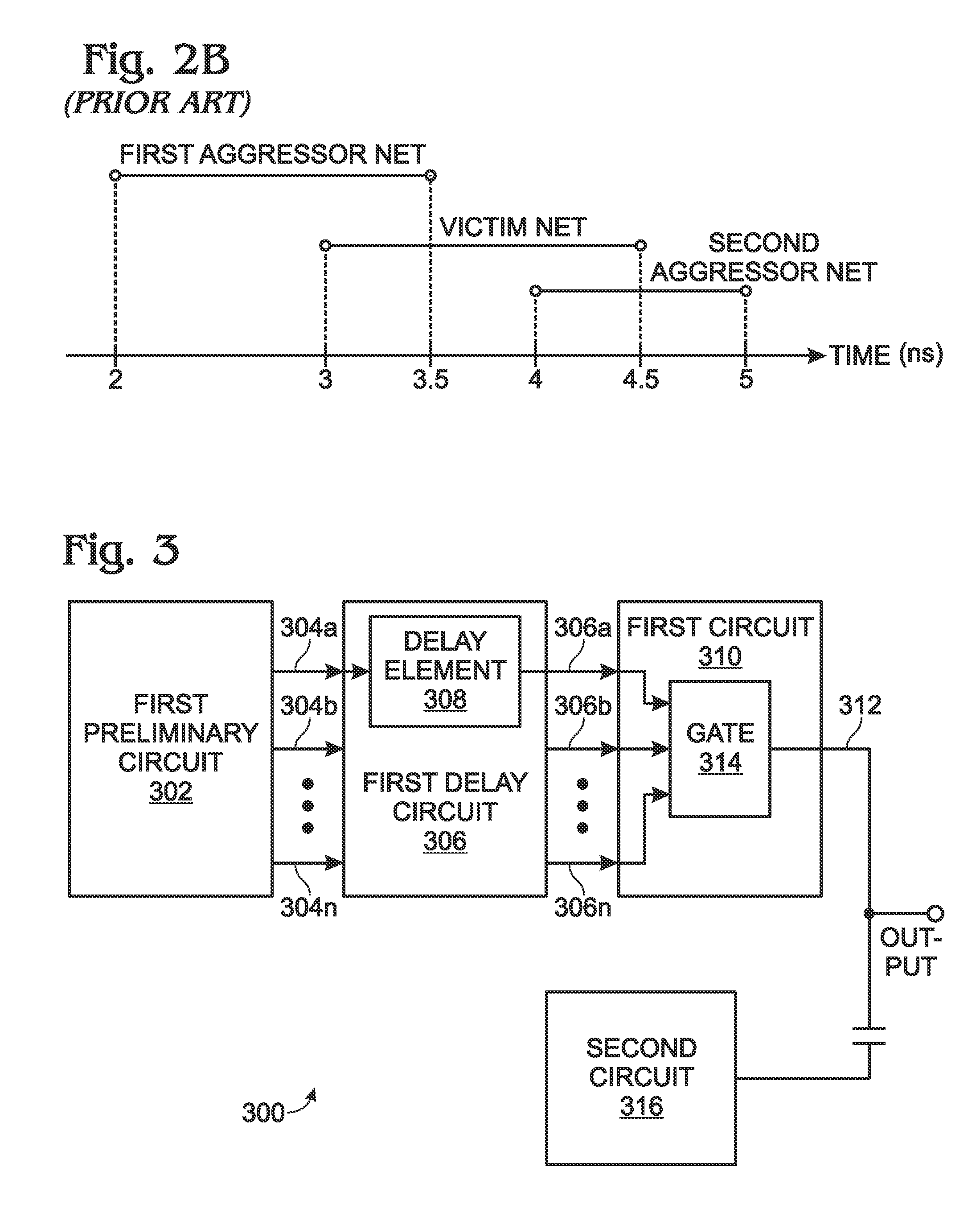
[0038]FIG. 3 is a schematic block diagram of a system of hardware devices connected with minimal signal crosstalk. The system 300 comprises a first preliminary circuit 302 having a first plurality of outputs 304 whose combination results in a preliminary net delay range (P) with a minimum delay (Pmin) and a maximum delay (Pmax), where (d1+P) at least partially overlaps aggressor net delay range (A1). Shown are outputs 304a through 304n, where n is a variable not limited to any particular value. A first delay circuit 306 has a first plurality of inputs 304 connected to the first preliminary circuit outputs, a first plurality of outputs 306 (306a through 306n). The first delay circuit 306 includes at least one delay element 308 with a delay (d) interposed between the first preliminary circuit minimum delay output (e.g., 304a) and the first delay circuit output 306a, resulting in a first shrunken net delay range with a minimum delay (Dmin) and a maximum delay (Dmax), where Dmin=d+Pmin,...


PUM


Abstract

A circuit analysis tool is provided, enabled with software instructions, for minimizing circuit crosstalk. The instructions provide a first circuit connected to an output mode, having a last gate with a plurality of inputs and an output. The instructions calculate a first circuit victim net delay range (timing window) having a minimum delay (Vmin) and a maximum delay (Vmax). A second circuit is provided having an output connected to the output node to supply an aggressor net delay range (A1) having a minimum delay (A1min) and a maximum delay (A1max). The aggressor net delay range at least partially overlaps the victim net delay range. Without increasing the value of Vmax (critical path timing), the first circuit victim net delay range is shrunk, thereby minimizing crosstalk between the first and second circuits without an increase in first circuit maximum signal delay.

Description

BACKGROUND OF THE INVENTION[0001]1. Field of the Invention[0002]This invention generally relates to signal networking and, more particularly, to a system and method for minimizing the susceptibility of a signal network to aggressor net timing window overlap.[0003]2. Description of the Related Art[0004]The size, complexity, and operating or switching speeds of semiconductor ICs have increased, while feature geometries have decreased, and interconnect systems for such ICs have dramatically increased in complexity. In many situations these factors have increased the possible impact on timing due to noise resulting from parasitic capacitance within the interconnect system.[0005]As noted in Wikipedia, in a synchronous digital system, data is supposed to move in lockstep, advancing one stage on each tick of the clock signal. This is enforced by synchronizing elements such as flip-flops or latches, which copy their input to their output when instructed to do so by the clock. To the first o...

Claims


Application Information

Patent Timeline
IPC IPC(8): G06F17/50
CPCG06F17/5031G06F17/5081G06F2217/82G06F2217/84G06F30/398G06F30/3312G06F2119/10G06F2119/12
Inventor SINGLA, SUNIL KUMARKOUL, SUDHIR
Owner MACOM CONNECTIVITY SOLUTIONS LLC
Why Eureka
Try Eureka