Inverse mode SiGe HBT cascode device and fabrication method

a cascode device and inverse mode technology, applied in the direction of transistors, solid-state devices, amplifier combinations, etc., can solve the problems of unwanted effects of semiconductor devices, lag in performance, and high cost of technologies, and the concept has only reached a sufficiently practical sta

a cascode device and inverse mode technology, applied in the direction of transistors, solid-state devices, amplifier combinations, etc., can solve the problems of unwanted effects of semiconductor devices, lag in performance, and high cost of technologies, and the concept has only reached a sufficiently practical sta

US8212291B2Inactive Publication Date: 2012-07-03GEORGIA TECH RES CORP

Image

  • Inverse mode SiGe HBT cascode device and fabrication method
  • Inverse mode SiGe HBT cascode device and fabrication method
  • Inverse mode SiGe HBT cascode device and fabrication method

Examples


Embodiment Construction

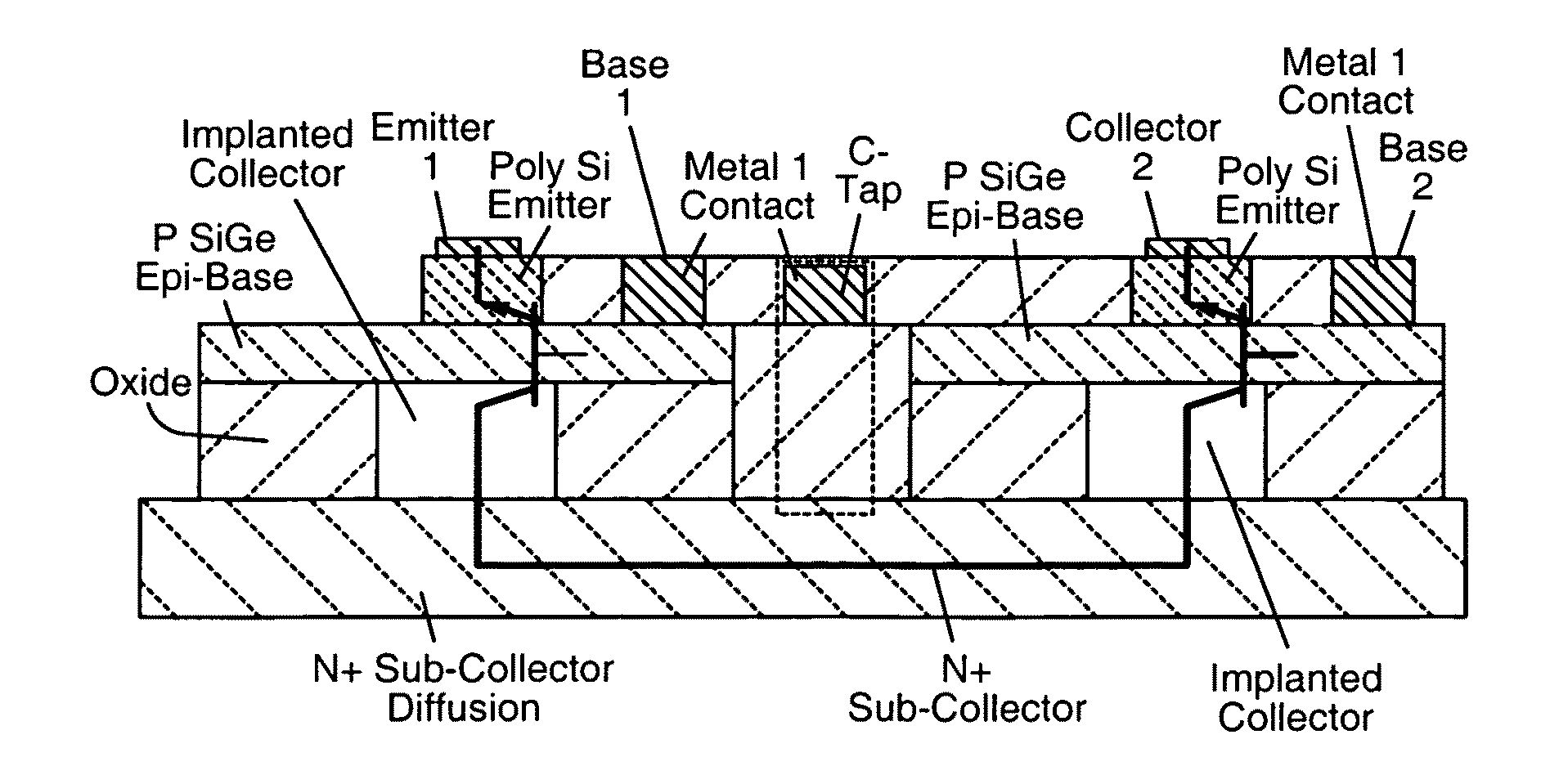
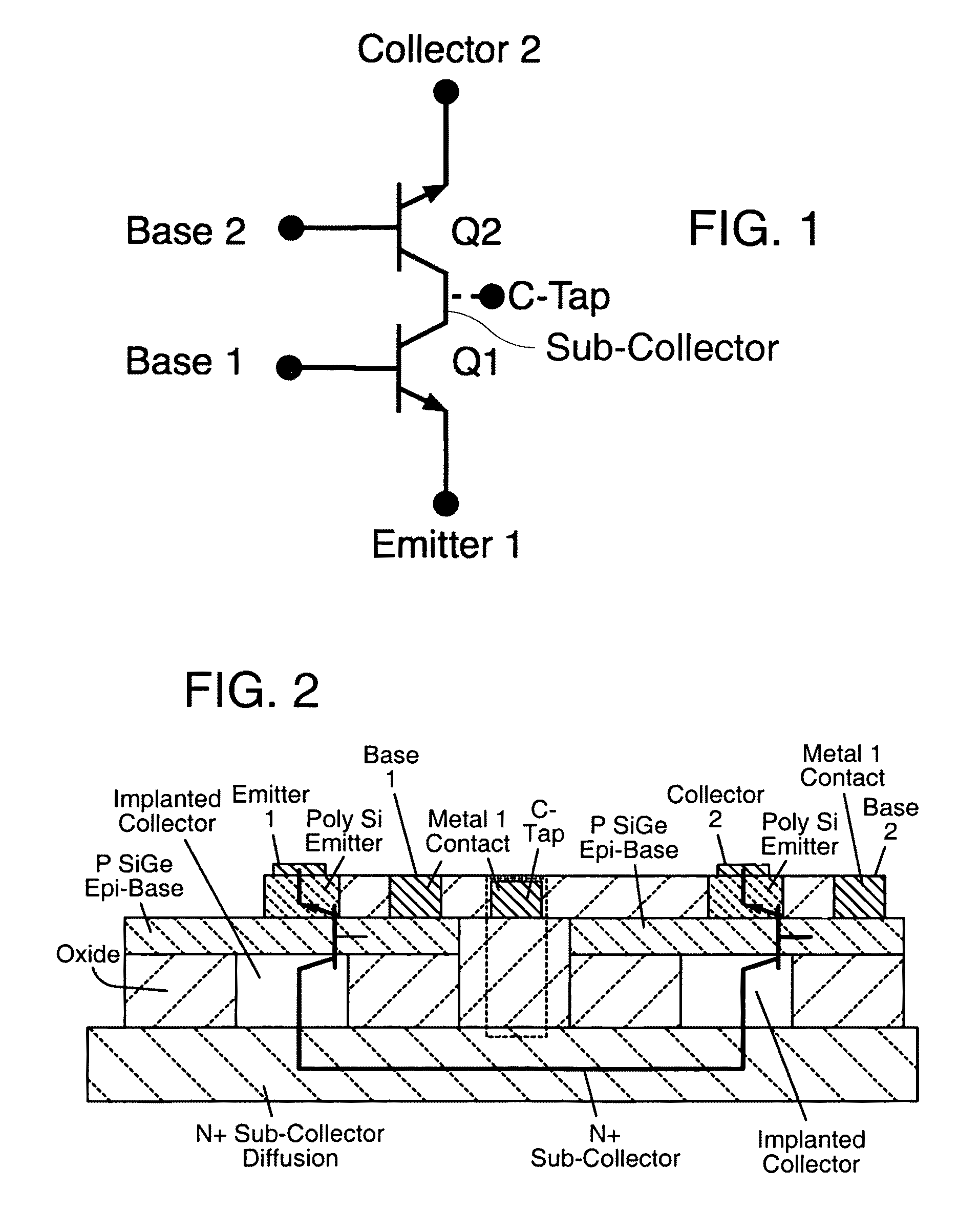
[0023]Briefly described, the present technology includes, in a preferred exemplary embodiment, a novel RHBD cascode topology comprising a forward-mode SiGe HBT sharing a sub-collector with an inverse-mode SiGe HBT. An electrical connection to the sub-collector may be present to provide additional SEU immunity. This topology can result in a device with smaller footprint and improved radiation hardening.

[0024]Referring now in greater detail to the drawings, in which like numerals represent like components throughout the several views, FIGS. 1-3 illustrate preferred embodiments of the inverse-mode cascode device.

[0025]FIG. 1 is a schematic of an exemplary inverse-mode cascode device or structure. As shown in FIG. 1, a first transistor, Q1 is operated as a common-emitter amplifier. A second transistor, Q2, is operated in unity-current-gain common-base mode. Given sufficient headroom (two VBE drops at minimum), the device may be operated as a standard single device with an input signal a...


PUM


Abstract

Disclosed is a device structure using an inverse-mode cascoded Silicon-Germanium (SiGe) Heterojunction Bipolar Transistor (HBT) beneficial in applications requiring radiation hardened circuitry. The device comprises a forward-mode common-emitter HBT cascoded with a common-base inverse-mode HBT, sharing a common sub-collector. An exemplary device was measured to have over 20 dB of current gain, and over 30 dB of power gain at 10 GHz, thus demonstrating the use of these circuits for high-frequency circuit applications. In addition, the radiation response and voltage limits were characterized and showed to have negligible performance effects in typical operating conditions. Due to the unique topology, the disclosed device has the benefit of being a more compact cascode design and the additional benefit of providing significantly improved radiation tolerance.

Description

[0001]This application claims the benefit of U.S. Provisional Application No. 61 / 035,903, filed Mar. 12, 2008.FIELD OF THE INVENTION[0002]The present invention relates generally to the field of semiconductor heterojunction bipolar transistors, and more particularly to a device structure and fabrication method using an inverse-mode cascoded SiGe HBT in which single-event-upset (SEU) hardening may be substantially improved.BACKGROUND OF THE INVENTION[0003]Space remains a classic extreme environment encompassing large radiation fields in addition to wide temperature swings; these environmental factors place stringent demands on technology platforms for use in space-based electronic systems.[0004]Ionizing radiation can cause unwanted effects in semiconductor devices. These unwanted changes of state caused by ions or electromagnetic radiation striking a sensitive node in a micro-electronic device are known as single event upsets (SEUs). SEU mitigation is a major concern and an area of ac...

Claims


Application Information

Patent Timeline
03 Jul 2012
Publication
US8212291B2
IPC
H01L29/737
CPC
H01L27/0744; H01L29/7378
Inventors
THRIVIKRAMAN, TUSHAR K.; APPASWAMY, ARAVIND