
Image sensor and method for manufacturing the same

a technology of image sensor and manufacturing method, applied in the field of image sensor, can solve the problems of image quality reduction, image defect generation, and charge sharing phenomenon,

Inactive Publication Date: 2012-07-17
DONGBU HITEK CO LTD
View PDF8 Cites 2 Cited by
  • Summary
  • Abstract
  • Description
  • Claims
  • Application Information

AI Technical Summary

Benefits of technology

This approach enhances image sensor performance by increasing the fill factor, minimizing dark current, and preventing sensitivity degradation, thereby improving image quality and reducing defects.

Problems solved by technology

As the size of a photodiode is reduced for the purpose of increasing the number of pixels without increasing chip size, the area of a light receiving portion is also reduced, thereby resulting in a reduction in image quality.
In the manufacture of a 3D image sensor according to a related-art, there are difficulties in performing a wafer-to wafer alignment between a photodiode positioned at an upper part of a chip and a readout circuit unit formed in a silicon substrate, and ensuring an ohmic contact due to a poor contact between an interconnection of the readout circuit unit and the photodiode.
Also, there is a limitation in that an image defect is generated by damage to an image sensing device such as an etching damage because a pixel isolation region is formed by using a device isolation layer in a related-art.
According to a related-art, there is a limitation in that a charge sharing phenomenon may occur because both the source and the drain of the transfer transistor are heavily doped with N-type impurities.
The charge sharing phenomenon may cause reduction of the sensitivity of an output image and generation of image error.
Also, photo charges may not smoothly move between a photodiode and a readout circuitry, causing generation of a dark current and reduction of saturation and sensitivity.

Method used


Image

  • Image sensor and method for manufacturing the same
  • Image sensor and method for manufacturing the same
  • Image sensor and method for manufacturing the same

Examples


first embodiment

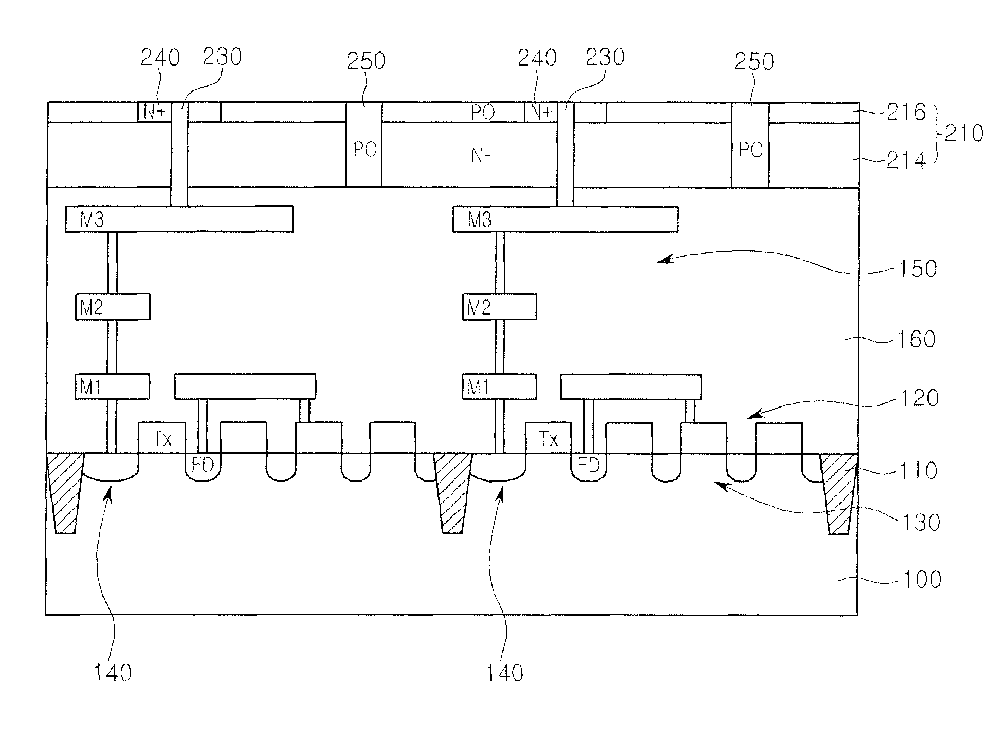
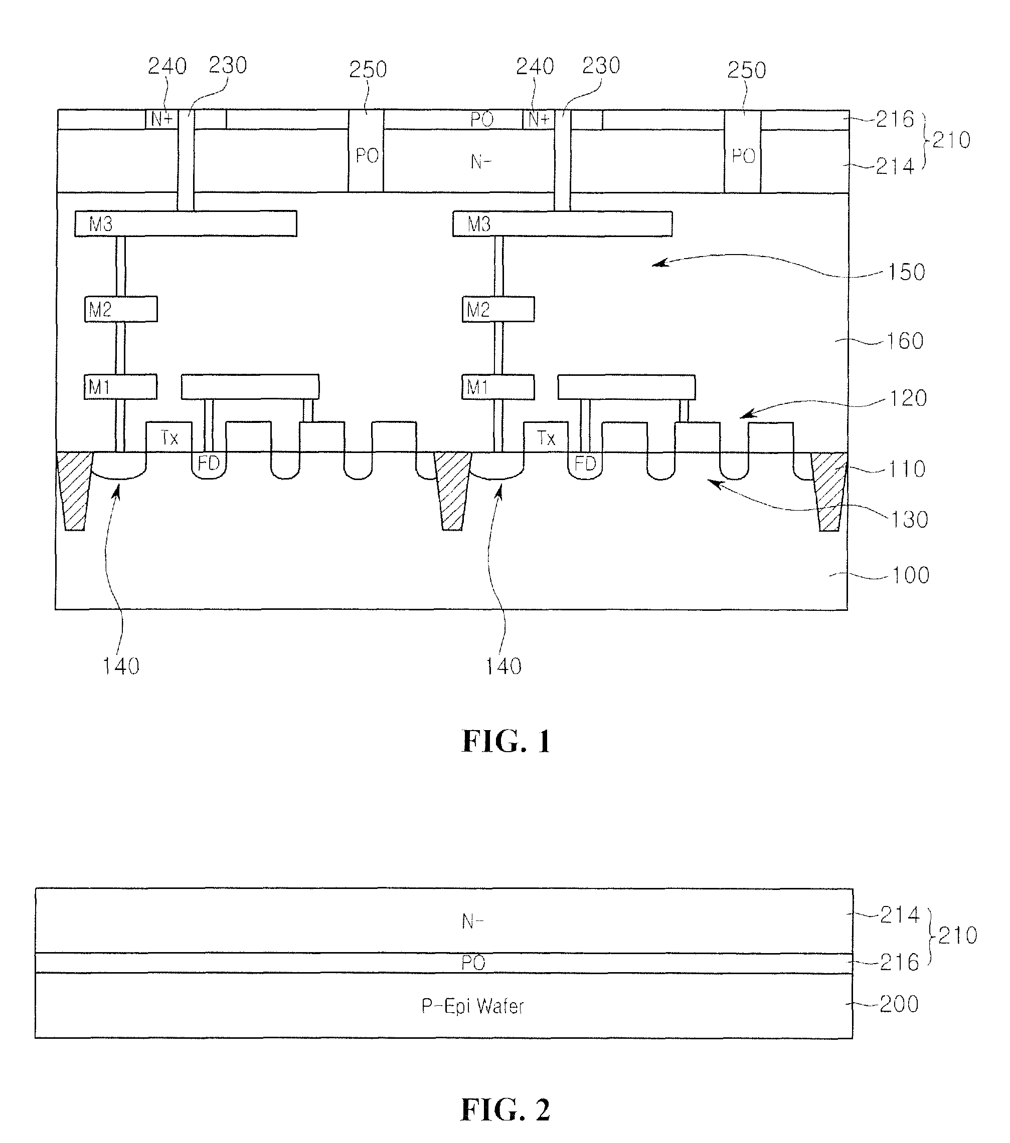
[0022]FIG. 1 is a cross-section view of an image sensor according to a

[0023]Referring to FIG. 1, an image sensor may include: a readout circuitry 120 in a first substrate 100; an interconnection 150 over the first substrate 100, the interconnection 150 being electrically connected to the readout circuitry 120; an image sensing device 210 over the interconnection 150, the image sensing device 210 including a first conductive-type conductive layer 214 and a second conductive-type conductive layer 216; a first conductive-type ion implantation layer 240 in a portion of the second conductive-type conductive layer 216 of the image sensing device 210; and a via plug 230 penetrating through the first conductive-type ion implantation layer 240 and connecting the first conductive-type conductive layer 214 to the interconnection 150.

[0024]The image sensing device 210 may be a photodiode, but, without being limited thereto, may be a photogate, or a combination of the photodiode and the photogat...

second embodiment

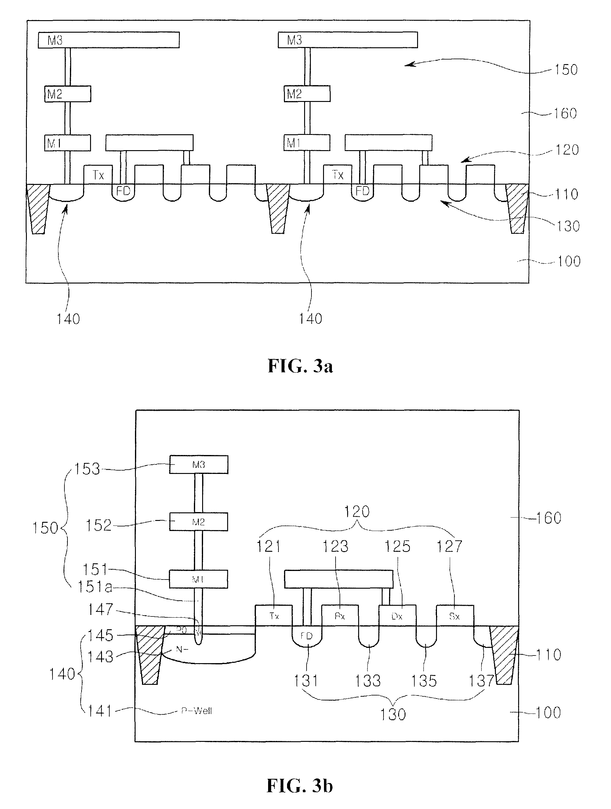
[0052]FIG. 9 is a cross-sectional view of an image sensor and is a detailed view of a first substrate 100 where a readout circuitry 120, an electrical junction region 140, and an interconnection 150 are formed.

[0053]The second embodiment may adopt the technical features of the first embodiment.

[0054]In the second embodiment unlike the first embodiment, a first conductive-type connection 148 is formed at one side of the electrical junction region 140.

[0055]An N+ connection region 148 may be formed at a P0 / N− / P− junction 140 for an ohmic contact. A process of forming an N+ connection region and a first metal contact 151a may provide a leakage source. This is because an electric field (EF) may be generated over the Si surface due to operation while a reverse bias is applied to P0 / N− / P− junction 140. A crystal defect generated during the contact forming process inside the electric field may become a leakage source.

[0056]Also, when the N+ connection region is formed over the surface of ...


PUM


Abstract

Provided are an image sensor and a method for manufacturing the same. The image sensor comprises a readout circuitry, an interconnection, an image sensing device, a first conductive-type ion implantation layer, and a via plug. The readout circuitry is formed in a first substrate. The interconnection is formed over the first substrate. The interconnection is electrically connected to the readout circuitry. Then image sensing device is formed over the interconnection. The image sensing device comprises a first conductive-type conductive layer and a second conductive-type conductive layer. The first conductive-type ion implantation layer is formed in a portion of the second conductive-type conductive layer of the image sensing device. The via plug penetrates through the first conductive-type ion implantation layer and the first conductive-type conductive layer to electrically connect the first conductive-type conductive layer to the interconnection.

Description

CROSS-REFERENCE TO RELATED APPLICATION[0001]This application claims the benefit under 35 U.S.C. §119 of Korean Patent Application No. 10-2008-0128500, filed Dec. 17, 2008, which is hereby incorporated by reference in its entirety.BACKGROUND[0002]The present disclosure relates to an image sensor and a method for manufacturing the same.[0003]Image sensors are semiconductor devices which can convert optical images into electrical signals. Such image sensors can typically be classified as either a Charge Coupled Device (CCD) or a Complementary Metal Oxide Semiconductor (CMOS) Image Sensor (CIS).[0004]During the fabrication of image sensors, a photodiode may be formed in a substrate using ion implantation. As the size of a photodiode is reduced for the purpose of increasing the number of pixels without increasing chip size, the area of a light receiving portion is also reduced, thereby resulting in a reduction in image quality.[0005]Also, since a stack height does not reduce as much as t...

Claims


Application Information

Patent Timeline
Patent Type & Authority Patents(United States)
IPC IPC(8): H01J40/14H01L31/02H04N25/00
CPCH01L27/14632H01L27/14687H01L27/14643H01L27/146
Inventor SHIM, HEE SUNG
Owner DONGBU HITEK CO LTD
Learn More