

Semiconductor device
a technology of semiconductor devices and semiconductors, applied in semiconductor devices, semiconductor/solid-state device details, electrical devices, etc., can solve the problems of easy peeling of the interface between the resin around the through hole and the die pad, device breakage, etc., to improve the reliability of a power semiconductor module, reduce the resistance of parasitic inductance, and reduce the effect of wiring resistan
- Summary
- Abstract
- Description
- Claims
- Application Information
AI Technical Summary
Benefits of technology
Problems solved by technology
Method used
Image

Examples
first embodiment
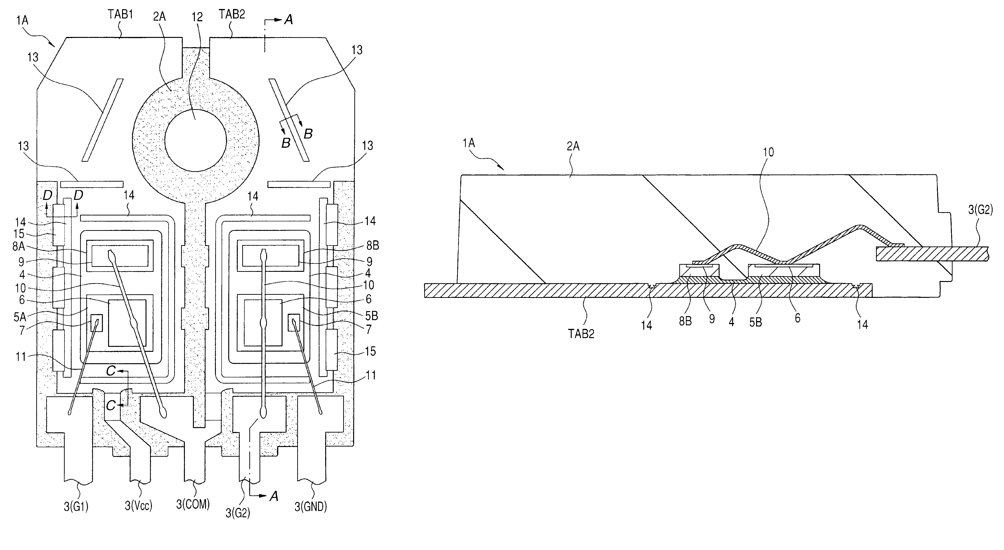
[0064]This embodiment concerns a semiconductor device applied to a switch module used in an inverter circuit for motor control.
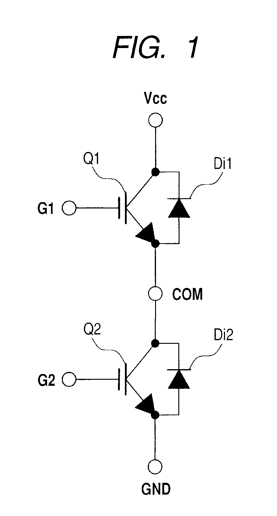
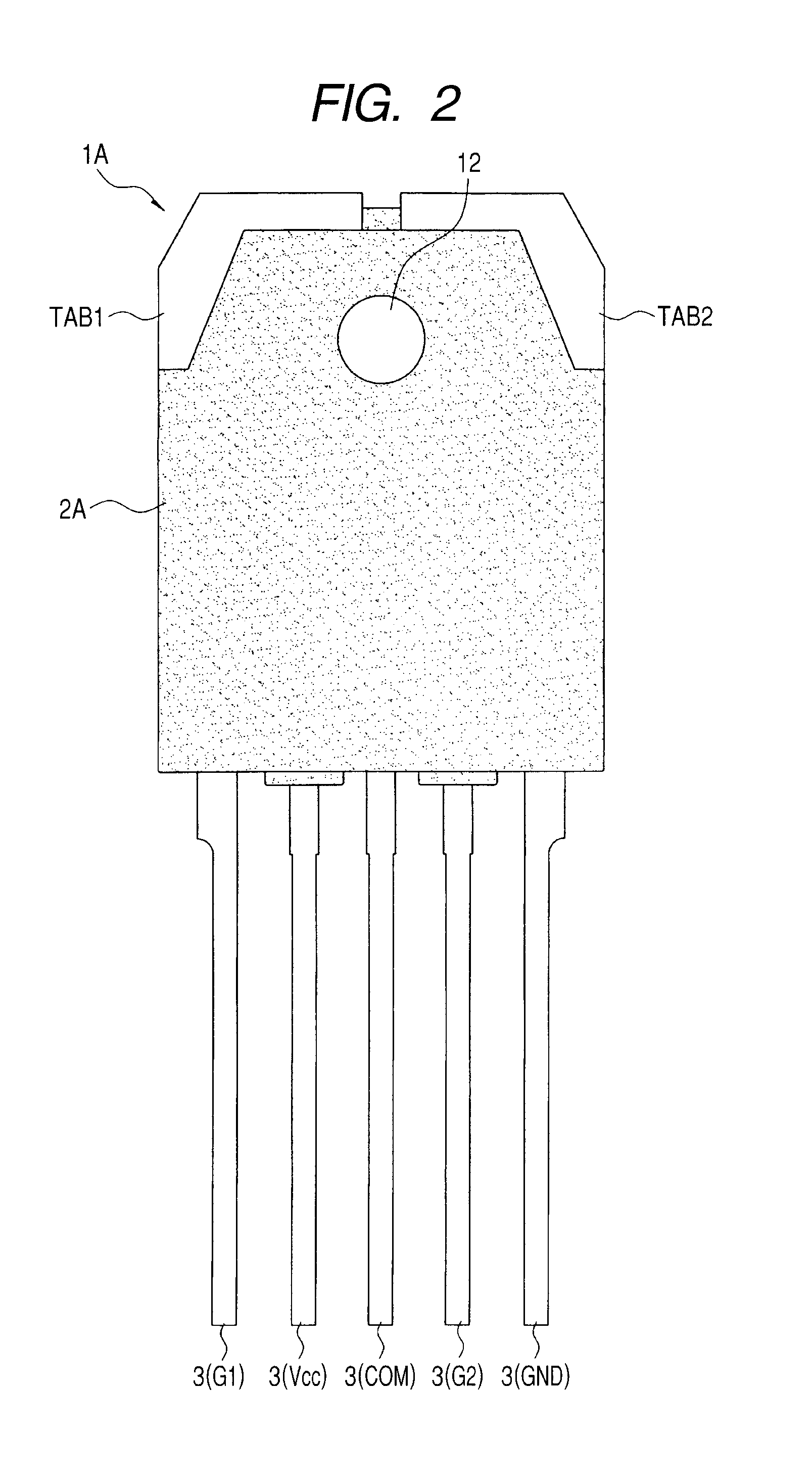
[0065]FIG. 1 shows the circuit configuration of a switch module according to this embodiment. The switch circuit includes a first semiconductor switch Q1, a second semiconductor switch Q2, a first diode Di1 and a second diode Di2 which are coupled between a pair of terminals (terminals Vcc and GND, or a power terminal and a ground terminal) serving as a current path. The first semiconductor switch Q1 and second semiconductor switch Q2 are each comprised of an IGBT (Insulated Gate Bipolar Transistor) and the first diode Di1 and second diode Di2 are each comprised of a fast recovery diode. The gate electrode of the first semiconductor switch Q1 and the gate electrode of the second semiconductor switch Q2 are coupled with terminal G1 and terminal G2 respectively and the emitter electrode of the first semiconductor switch Q1 and the collector electrode of the se...
second embodiment
[0107]FIG. 24 is a plan view showing the external appearance of the semiconductor package according to the second embodiment; FIG. 25 is a plan view showing the back side of the semiconductor package (on which the heat radiating plate is mounted); FIG. 26 is a side view of the semiconductor package; FIG. 27 is a plan view showing the internal structure of the semiconductor package; and FIG. 28 is a sectional view taken along the line E-E in FIG. 27.
[0108]Whereas the lower surfaces of the die pads (TAB1, TAB2) are exposed from the lower surface of the sealing body 2B in the semiconductor package 1A according to the first embodiment, the die pads (TAB1, TAB2) are completely covered by the sealing body 2A in the semiconductor package 1B according to the second embodiment.
[0109]Five leads 3 protruding in parallel from one lateral side of the sealing body 2B correspond to the five terminals of the switch circuit shown in FIG. 1 as in the first embodiment. Namely, the five leads 3 are as ...
PUM
 Abstract
Description
Claims
Application Information