Semiconductor device

a technology of semiconductor devices and power pins, applied in semiconductor devices, semiconductor/solid-state device details, electrical apparatus, etc., can solve the problems of increasing the size of the device, increasing the complexity of the device, so as to achieve the effect of efficiently preventing the noise of adjacent circuits due to massive currents when tsv acts as a power pin

Active Publication Date: 2012-07-24
MARLIN SEMICON LTD
View PDF6 Cites 10 Cited by
  • Summary
  • Abstract
  • Description
  • Claims
  • Application Information

AI Technical Summary

Benefits of technology

[0016]According to the novel shelter component disposed between the TSV and the circuit area, noise in adjacent circuits due to massive currents when TSV acts as a power pin can be efficiently prevented.

Problems solved by technology

With the development of technology and the increasingly imaginative applications of electrical products, the IC device is becoming smaller, more delicate and more diversified.
However, when the TSV 14 acts as a power pin, the current conducted through the metal interconnect layer 13 is massive, thereby causing serious electromagnetic interference (EMI) to adjacent circuits, for example, the metal interconnect circuit 13 or the circuit area 17 in area A. This is an urgent problem to be resolved.

Method used


Image

  • Semiconductor device
  • Semiconductor device
  • Semiconductor device

Examples


Embodiment Construction

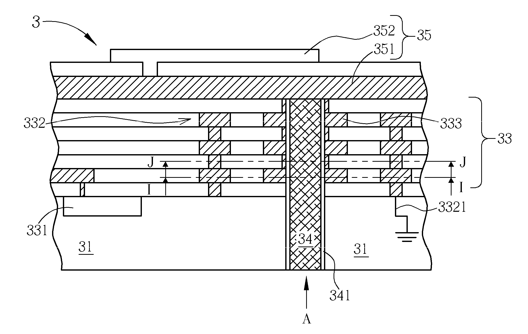
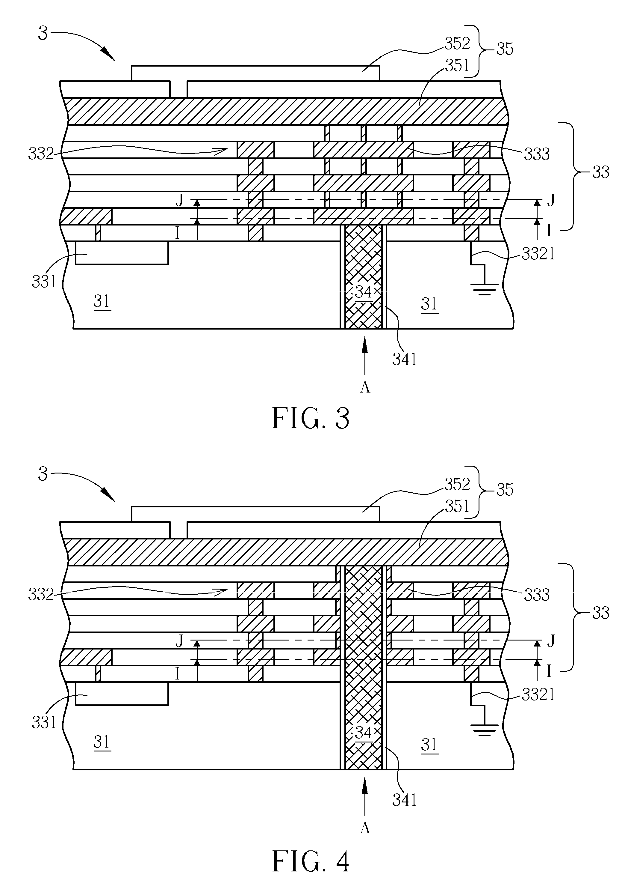
[0023]Referring to the words “up” or “down” that describe the relationship between components in the text, it is well known in the art and should be clearly understood that these words refer to relative positions that can be inverted to obtain a same structure, and these structures should therefore not be precluded from the scope of the claims in the present invention.

[0024]FIG. 3 illustrates the semiconductor device in the present invention. As shown in FIG. 3, the semiconductor device 3 in the present invention comprises a substrate 31, at least a TSV 34, a plurality of metal interconnect layers 33 and a circuit area 331. The substrate 31 is composed of single-crystalline silicon, gallium arsenide (GaAs) or other well-known material. The TSV 34 is disposed in the substrate 31 and penetrates through the substrate 31. The TSV 34 is composed of copper, polycrystalline silicon, tungsten, aluminum or other conductive material, and is wrapped by an insulation layer 341 to prevent leakag...


PUM


Abstract

A semiconductor device with a TSV and a shelter is provided. The semiconductor device includes a substrate, a circuit area, at least a TSV and a shelter. The circuit area and the TSV are disposed on the substrate, and the TSV penetrates through the substrate. The shelter is disposed on the substrate and at least one part thereof is between the circuit area and the TSV in order to shelter EMI between the TSV and the circuit area. The novel structure prevents the circuits in the circuit area being affected by noise caused by TSV when TSV acts as a power pin.

Description

BACKGROUND OF THE INVENTION[0001]1. Field of the Invention[0002]The present invention relates to a semiconductor device, and more particularly, to a semiconductor device with a TSV and a shelter.[0003]2. Description of the Prior Art[0004]In modern society, the micro-processor system comprised of integrated circuits (IC) is a ubiquitous device, being utilized in such diverse fields as automatic control electronics, mobile communication devices and personal computers. With the development of technology and the increasingly imaginative applications of electrical products, the IC device is becoming smaller, more delicate and more diversified.[0005]As is well known in the art, an IC device is produced from dies that are fabricated by conventional semiconductor manufacturing processes. The process to manufacture a die starts with a wafer: first, different regions are marked on the wafer; second, conventional semiconductor manufacture processes such as deposition, photolithography, etching...

Claims


Application Information

Patent Timeline
Patent Type & Authority Patents(United States)
IPC IPC(8): H01L21/762
CPCH01L23/481H01L23/552H01L25/0657H01L2225/06541H01L2224/16146H01L2224/131H01L2924/014H01L2224/05569H01L2224/05008H01L2224/05009H01L2224/05025H01L2224/05548H01L2224/05001H01L2224/05124H01L2224/05147H01L2224/05184H01L2224/05624H01L24/05H01L2924/00014
Inventor KUO, CHIEN-LI
Owner MARLIN SEMICON LTD
Why Eureka
Try Eureka